Koga Hirotaka, Nagashima Kazuki, Suematsu Koichi, Takahashi Tsunaki, Zhu Luting, Fukushima Daiki, Huang Yintong, Nakagawa Ryo, Liu Jiangyang, Uetani Kojiro, Nogi Masaya, Yanagida Takeshi, Nishina Yuta
SANKEN (The Institute of Scientific and Industrial Research), Osaka University, 8-1 Mihogaoka, Ibaraki, Osaka 567-0047, Japan.
Department of Applied Chemistry, Graduate School of Engineering, The University of Tokyo, 7-3-1 Hongo, Bunkyo-ku, Tokyo 113-8656, Japan.
ACS Nano. 2022 Jun 28;16(6):8630-8640. doi: 10.1021/acsnano.1c10728. Epub 2022 Apr 26.
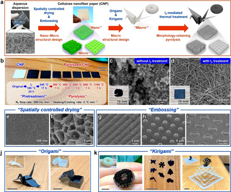
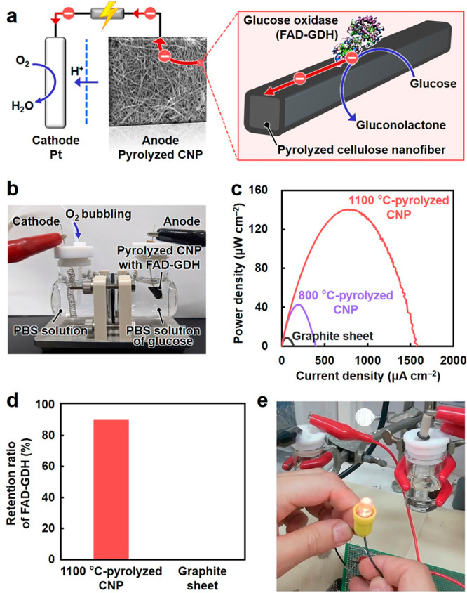
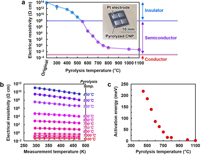
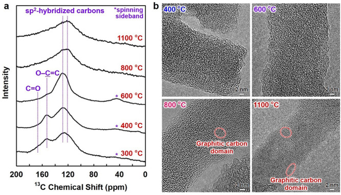
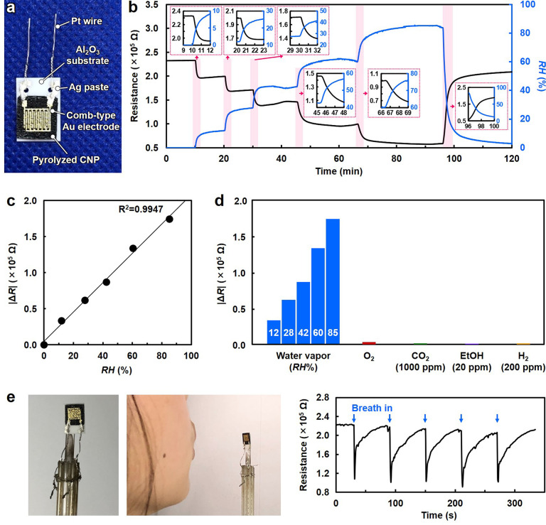
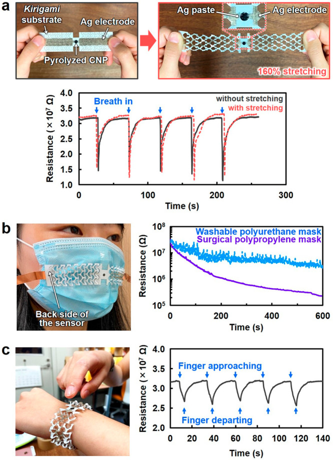
Semiconducting nanomaterials with 3D network structures exhibit various fascinating properties such as electrical conduction, high permeability, and large surface areas, which are beneficial for adsorption, separation, and sensing applications. However, research on these materials is substantially restricted by the limited trans-scalability of their structural design and tunability of electrical conductivity. To overcome this challenge, a pyrolyzed cellulose nanofiber paper (CNP) semiconductor with a 3D network structure is proposed. Its nano-micro-macro trans-scale structural design is achieved by a combination of iodine-mediated morphology-retaining pyrolysis with spatially controlled drying of a cellulose nanofiber dispersion and paper-crafting techniques, such as microembossing, , and . The electrical conduction of this semiconductor is widely and systematically tuned, the temperature-controlled progressive pyrolysis of CNP, from insulating (10 Ω cm) to quasimetallic (10 Ω cm), which considerably exceeds that attained in other previously reported nanomaterials with 3D networks. The pyrolyzed CNP semiconductor provides not only the tailorable functionality for applications ranging from water-vapor-selective sensors to enzymatic biofuel cell electrodes but also the designability of macroscopic device configurations for stretchable and wearable applications. This study provides a pathway to realize structurally and functionally designable semiconducting nanomaterials and all-nanocellulose semiconducting technology for diverse electronics.
具有三维网络结构的半导体纳米材料展现出各种迷人的特性,如导电性、高渗透性和大表面积,这些特性有利于吸附、分离和传感应用。然而,对这些材料的研究在很大程度上受到其结构设计的有限跨尺度可扩展性和电导率可调性的限制。为了克服这一挑战,提出了一种具有三维网络结构的热解纤维素纳米纤维纸(CNP)半导体。其纳米-微米-宏观跨尺度结构设计是通过碘介导的形态保留热解与纤维素纳米纤维分散体的空间控制干燥以及诸如微压花等造纸技术相结合来实现的。这种半导体的导电性通过对CNP进行温度控制的渐进热解得到广泛而系统的调节,从绝缘(10Ω·cm)到准金属(10Ω·cm),这大大超过了其他先前报道的具有三维网络的纳米材料所达到的水平。热解后的CNP半导体不仅为从水蒸气选择性传感器到酶生物燃料电池电极等各种应用提供了可定制的功能,还为可拉伸和可穿戴应用提供了宏观器件配置的可设计性。这项研究为实现结构和功能可设计的半导体纳米材料以及用于各种电子产品的全纳米纤维素半导体技术提供了一条途径。