Wang Zhiwei, Dai Jie, Wang Jian, Li Xinzhe, Pei Chengjie, Liu Yanlei, Yan Jiaxu, Wang Lin, Li Shaozhou, Li Hai, Wang Xiaoshan, Huang Xiao, Huang Wei
Institute of Advanced Materials (IAM), Nanjing Tech University (NanjingTech), 30 South Puzhu Road, Nanjing 211816, China.
Frontiers Science Center for Flexible Electronics, Xi'an Institute of Flexible Electronics (IFE) and Xi'an Institute of Biomedical Materials & Engineering, Northwestern Polytechnical University, 127 West Youyi Road, Xi'an 710072, China.
Research (Wash D C). 2022 Jun 23;2022:9767651. doi: 10.34133/2022/9767651. eCollection 2022.
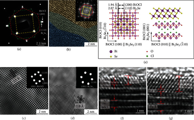
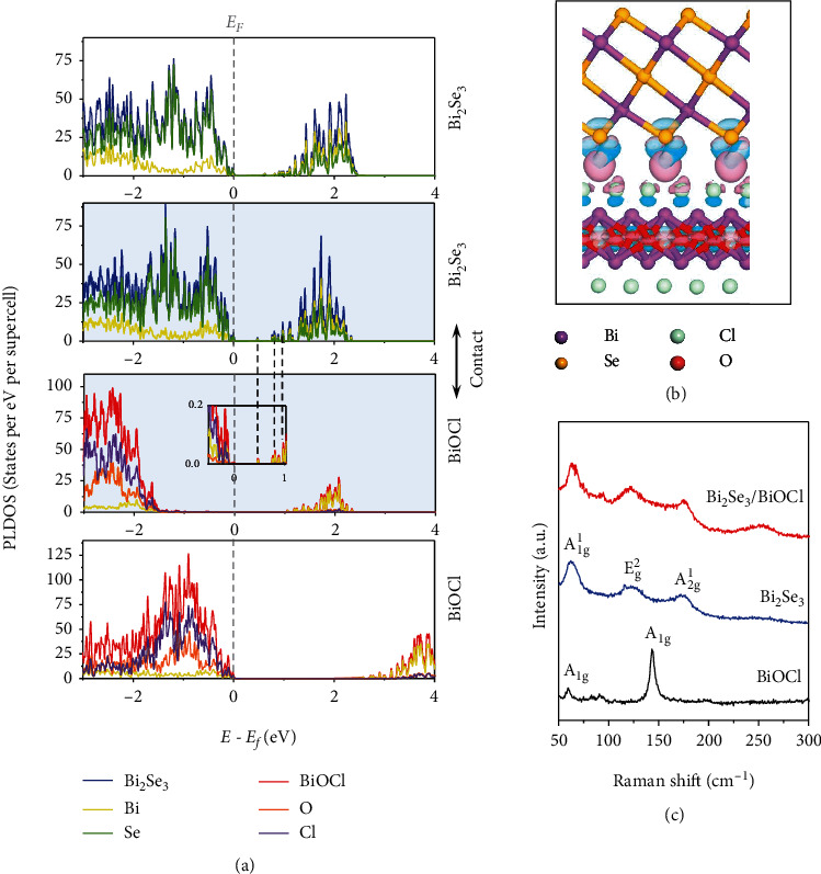
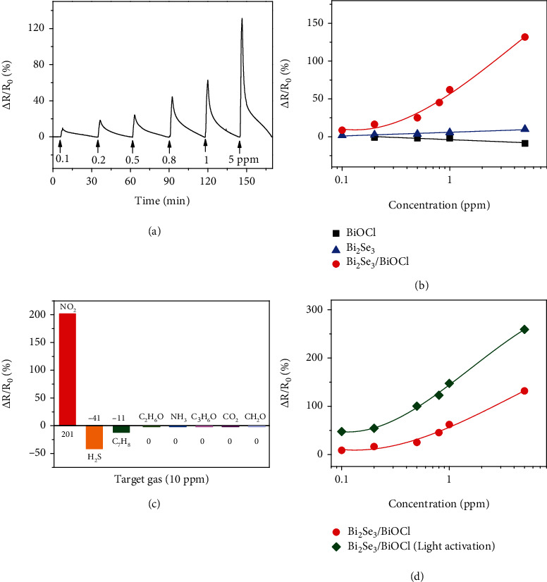
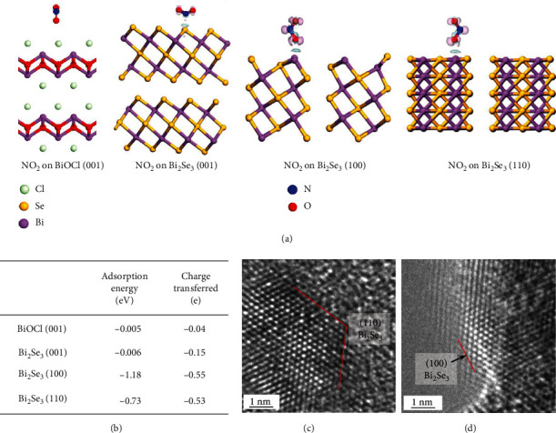
Most van der Waals two-dimensional (2D) materials without surface dangling bonds show limited surface activities except for their edge sites. Ultrathin BiSe, a topological insulator that behaves metal-like under ambient conditions, has been overlooked on its surface activities. Herein, through a topochemical conversion process, ultrathin nanoporous BiSe layers were epitaxially deposited on BiOCl nanosheets with strong electronic coupling, leading to hybrid electronic states with further bandgap narrowing. Such oriented nanoporous BiSe layers possessed largely exposed active edge sites, along with improved surface roughness and film forming ability even on inkjet-printed flexible electrodes. Superior room-temperature NO sensing performance was achieved compared to other 2D materials under bent conditions. Our work demonstrates that creating nanoscale features in 2D materials through topochemical heteroepitaxy is promising to achieve both favorable electronic properties and surface activity toward practical applications.
除边缘位点外,大多数没有表面悬空键的范德华二维(2D)材料的表面活性有限。超薄BiSe是一种在环境条件下表现出类金属行为的拓扑绝缘体,其表面活性一直被忽视。在此,通过一种拓扑化学转化过程,超薄纳米多孔BiSe层外延沉积在具有强电子耦合的BiOCl纳米片上,导致混合电子态并进一步使带隙变窄。这种取向的纳米多孔BiSe层具有大量暴露的活性边缘位点,即使在喷墨打印的柔性电极上也具有改善的表面粗糙度和成膜能力。与其他二维材料相比,在弯曲条件下实现了优异的室温NO传感性能。我们的工作表明,通过拓扑化学异质外延在二维材料中创建纳米级特征有望实现良好的电子性能和面向实际应用的表面活性。