• 文献检索
  • 文档翻译
  • 深度研究
  • 学术资讯
  • Suppr Zotero 插件Zotero 插件
  • 邀请有礼
  • 套餐&价格
  • 历史记录
应用&插件
Suppr Zotero 插件Zotero 插件浏览器插件Mac 客户端Windows 客户端微信小程序
定价
高级版会员购买积分包购买API积分包
服务
文献检索文档翻译深度研究API 文档MCP 服务
关于我们
关于 Suppr公司介绍联系我们用户协议隐私条款
关注我们

Suppr 超能文献

核心技术专利:CN118964589B侵权必究
粤ICP备2023148730 号-1Suppr @ 2026

文献检索

告别复杂PubMed语法,用中文像聊天一样搜索,搜遍4000万医学文献。AI智能推荐,让科研检索更轻松。

立即免费搜索

文件翻译

保留排版,准确专业,支持PDF/Word/PPT等文件格式,支持 12+语言互译。

免费翻译文档

深度研究

AI帮你快速写综述,25分钟生成高质量综述,智能提取关键信息,辅助科研写作。

立即免费体验

基于氧化锌的无序薄膜晶体管的亚阈值传导

Subthreshold Conduction of Disordered ZnO-Based Thin-Film Transistors.

作者信息

Yoon Minho

机构信息

Department of Physics and Institute of Quantum Convergence Technology, Kangwon National University, Chuncheon 24341, Republic of Korea.

出版信息

Micromachines (Basel). 2023 Aug 13;14(8):1596. doi: 10.3390/mi14081596.

DOI:10.3390/mi14081596
PMID:37630132
原文链接:https://pmc.ncbi.nlm.nih.gov/articles/PMC10456918/
Abstract

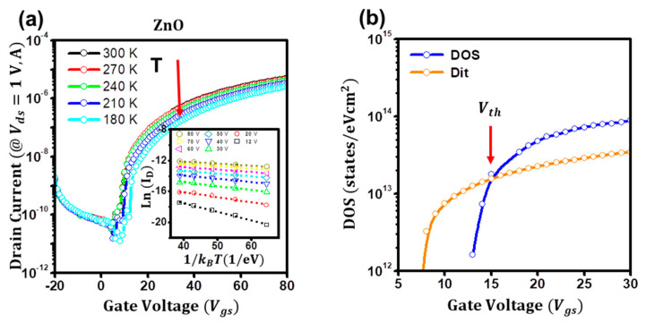
This study presents the disorderedness effects on the subthreshold characteristics of atomically deposited ZnO thin-film transistors (TFTs). Bottom-gate ZnO TFTs show n-type enhancement-mode transfer characteristics but a gate-voltage-dependent, degradable subthreshold swing. The charge-transport characteristics of the disordered semiconductor TFTs are severely affected by the localized trap states. Thus, we posit that the disorderedness factors, which are the interface trap capacitance and the diffusion coefficient of electrons, would result in the degradation. Considering the factors as gate-dependent power laws, we derive the subthreshold current-voltage relationship for disordered semiconductors. Notably, the gate-dependent disorderedness parameters are successfully deduced and consistent with those obtained by the / method, which was for the FinFETs. In addition, temperature-dependent current-voltage analyses reveal that the gate-dependent interface traps limit the subthreshold conduction, leading to the diffusion current. Thus, we conclude that the disorderedness factors of the ZnO films lead to the indefinable subthreshold swing of the ZnO TFTs.

摘要

本研究展示了无序性对原子沉积氧化锌薄膜晶体管(TFT)亚阈值特性的影响。底栅氧化锌TFT呈现n型增强模式转移特性,但具有与栅极电压相关的、可降解的亚阈值摆幅。无序半导体TFT的电荷传输特性受到局部陷阱态的严重影响。因此,我们假定无序性因素,即界面陷阱电容和电子扩散系数,会导致这种降解。将这些因素视为与栅极相关的幂律,我们推导出了无序半导体的亚阈值电流-电压关系。值得注意的是,成功推导出了与栅极相关的无序性参数,且这些参数与通过用于鳍式场效应晶体管(FinFET)的/方法获得的参数一致。此外,温度相关的电流-电压分析表明,与栅极相关的界面陷阱限制了亚阈值传导,导致扩散电流。因此,我们得出结论,氧化锌薄膜的无序性因素导致了氧化锌TFT难以确定的亚阈值摆幅。

https://cdn.ncbi.nlm.nih.gov/pmc/blobs/a7b3/10456918/c0fafbc10a1c/micromachines-14-01596-g005.jpg
https://cdn.ncbi.nlm.nih.gov/pmc/blobs/a7b3/10456918/dc54acd20b06/micromachines-14-01596-g001.jpg
https://cdn.ncbi.nlm.nih.gov/pmc/blobs/a7b3/10456918/adc0157eb9d2/micromachines-14-01596-g002.jpg
https://cdn.ncbi.nlm.nih.gov/pmc/blobs/a7b3/10456918/0b95a419afce/micromachines-14-01596-g003.jpg
https://cdn.ncbi.nlm.nih.gov/pmc/blobs/a7b3/10456918/7301c23ce0f1/micromachines-14-01596-g004.jpg
https://cdn.ncbi.nlm.nih.gov/pmc/blobs/a7b3/10456918/c0fafbc10a1c/micromachines-14-01596-g005.jpg

相似文献

1
Subthreshold Conduction of Disordered ZnO-Based Thin-Film Transistors.基于氧化锌的无序薄膜晶体管的亚阈值传导
Micromachines (Basel). 2023 Aug 13;14(8):1596. doi: 10.3390/mi14081596.
2
Threshold-Voltage Extraction Methods for Atomically Deposited Disordered ZnO Thin-Film Transistors.用于原子沉积无序氧化锌薄膜晶体管的阈值电压提取方法
Materials (Basel). 2023 Apr 7;16(8):2940. doi: 10.3390/ma16082940.
3
Low-voltage operation of ZrO2-gated n-type thin-film transistors based on a channel formed by hybrid phases of SnO and SnO2.基于由SnO和SnO2混合相形成的沟道的ZrO2栅控n型薄膜晶体管的低压操作。
ACS Appl Mater Interfaces. 2015 Jul 22;7(28):15129-37. doi: 10.1021/acsami.5b02941. Epub 2015 Jul 13.
4
Approaching subthreshold-swing limit for thin-film transistors by using a giant-dielectric-constant gate dielectric.通过使用高介电常数栅极电介质逼近薄膜晶体管的亚阈值摆幅极限。
RSC Adv. 2019 Aug 28;9(46):27117-27124. doi: 10.1039/c9ra03574e. eCollection 2019 Aug 23.
5
Lowering the Trap-State Density of Transparent Amorphous Oxide Semiconductor-Based Thin Film Transistors Through Microwave Irradiation.通过微波辐照降低基于透明非晶氧化物半导体的薄膜晶体管的陷阱态密度
J Nanosci Nanotechnol. 2020 Nov 1;20(11):6920-6924. doi: 10.1166/jnn.2020.18811.
6
Structural Engineering Effects on Hump Characteristics of ZnO/InSnO Heterojunction Thin-Film Transistors.结构工程对ZnO/InSnO异质结薄膜晶体管驼峰特性的影响
Nanomaterials (Basel). 2022 Mar 31;12(7):1167. doi: 10.3390/nano12071167.
7
High performance thin film transistor with ZnO channel layer deposited by DC magnetron sputtering.具有通过直流磁控溅射沉积的ZnO沟道层的高性能薄膜晶体管。
J Nanosci Nanotechnol. 2008 Sep;8(9):4557-60. doi: 10.1166/jnn.2008.ic24.
8
Dual-gate low-voltage transparent electric-double-layer thin-film transistors with a top gate for threshold voltage modulation.具有用于阈值电压调制的顶栅的双栅极低压透明电双层薄膜晶体管。
RSC Adv. 2020 Mar 3;10(14):8093-8096. doi: 10.1039/c9ra10619g. eCollection 2020 Feb 24.
9
Rational Design of ZnO:H/ZnO Bilayer Structure for High-Performance Thin-Film Transistors.ZnO:H/ZnO 双层结构的理性设计用于高性能薄膜晶体管。
ACS Appl Mater Interfaces. 2016 Mar;8(12):7862-8. doi: 10.1021/acsami.5b10778. Epub 2016 Mar 15.
10
An Analytical Model for Dual Gate Piezoelectrically Sensitive ZnO Thin Film Transistors.双栅压电敏感ZnO薄膜晶体管的解析模型
Adv Mater Technol. 2021 Aug;6(8). doi: 10.1002/admt.202100224. Epub 2021 Jun 24.

引用本文的文献

1
Effect of Deposition Temperature on Zn Interstitials and Oxygen Vacancies in RF-Sputtered ZnO Thin Films and Thin Film-Transistors.沉积温度对射频溅射ZnO薄膜及薄膜晶体管中锌间隙原子和氧空位的影响
Materials (Basel). 2024 Oct 23;17(21):5153. doi: 10.3390/ma17215153.

本文引用的文献

1
Threshold-Voltage Extraction Methods for Atomically Deposited Disordered ZnO Thin-Film Transistors.用于原子沉积无序氧化锌薄膜晶体管的阈值电压提取方法
Materials (Basel). 2023 Apr 7;16(8):2940. doi: 10.3390/ma16082940.
2
Nanospike electrodes and charge nanoribbons: A new design for nanoscale thin-film transistors.纳米尖峰电极和电荷纳米带:纳米级薄膜晶体管的一种新设计。
Sci Adv. 2022 Jan 28;8(4):eabm1154. doi: 10.1126/sciadv.abm1154.
3
Self-Assembled Nanodielectrics for Solution-Processed Top-Gate Amorphous IGZO Thin-Film Transistors.
用于溶液处理顶栅非晶铟镓锌氧化物薄膜晶体管的自组装纳米电介质
ACS Appl Mater Interfaces. 2021 Apr 7;13(13):15399-15408. doi: 10.1021/acsami.1c00249. Epub 2021 Mar 29.
4
Flexible indium-gallium-zinc-oxide Schottky diode operating beyond 2.45 GHz.工作频率超过 2.45GHz 的柔性铟镓锌氧化物肖特基二极管。
Nat Commun. 2015 Jul 3;6:7561. doi: 10.1038/ncomms8561.
5
Low-power flexible organic light-emitting diode display device.低功耗柔性有机发光二极管显示装置
Adv Mater. 2011 Aug 16;23(31):3511-6. doi: 10.1002/adma.201101066. Epub 2011 Jul 7.
6
Materials and mechanics for stretchable electronics.可拉伸电子产品的材料与力学
Science. 2010 Mar 26;327(5973):1603-7. doi: 10.1126/science.1182383.