Materials Sciences Division, Lawrence Berkeley National Laboratory, Berkeley, California 94720, USA.
Nat Commun. 2011;2:249. doi: 10.1038/ncomms1249.
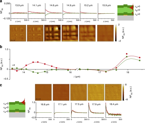
A planar slab of negative-index material works as a superlens with sub-diffraction-limited resolution, as propagating waves are focused and, moreover, evanescent waves are reconstructed in the image plane. Here we demonstrate a superlens for electric evanescent fields with low losses using perovskites in the mid-infrared regime. The combination of near-field microscopy with a tunable free-electron laser allows us to address precisely the polariton modes, which are critical for super-resolution imaging. We spectrally study the lateral and vertical distributions of evanescent waves around the image plane of such a lens, and achieve imaging resolution of λ/14 at the superlensing wavelength. Interestingly, at certain distances between the probe and sample surface, we observe a maximum of these evanescent fields. Comparisons with numerical simulations indicate that this maximum originates from an enhanced coupling between probe and object, which might be applicable for multifunctional circuits, infrared spectroscopy and thermal sensors.
负折射率材料的平板可作为超透镜,实现亚衍射极限分辨率,因为传播波被聚焦,而且,消逝波在像平面中被重建。在这里,我们使用中红外范围内的钙钛矿展示了用于电消逝场的低损耗超透镜。近场显微镜与可调谐自由电子激光的结合使我们能够精确地解决对于超分辨率成像至关重要的极化激元模式。我们对这种透镜的像平面周围的消逝波的横向和纵向分布进行了光谱研究,并在超透镜波长处实现了 λ/14 的成像分辨率。有趣的是,在探针和样品表面之间的某些距离处,我们观察到这些消逝场的最大值。与数值模拟的比较表明,这种最大值源自探针和物体之间的增强耦合,这可能适用于多功能电路、红外光谱和热传感器。