Department of Information Materials Science and Technology, Harbin Institute of Technology, Harbin, 150001, China.
Nanoscale Res Lett. 2012 Nov 26;7(1):649. doi: 10.1186/1556-276X-7-649.
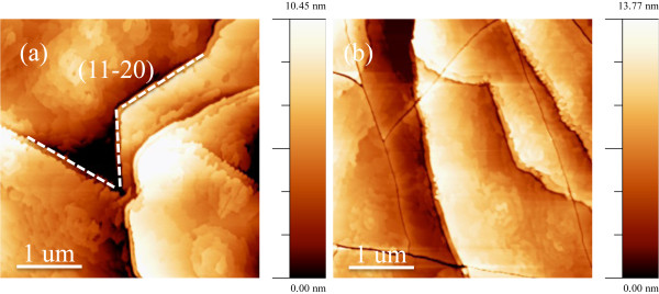
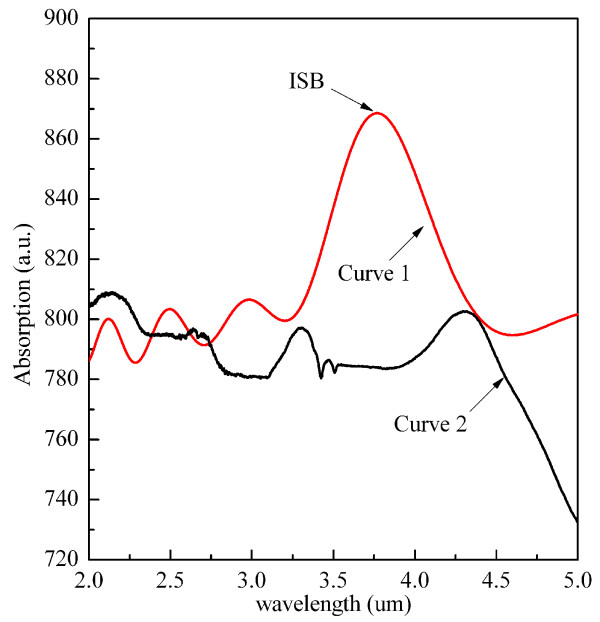
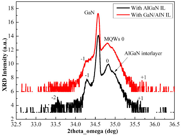
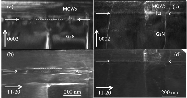
High Al content AlxGa1-xN/GaN multiple quantum well (MQW) films with different interlayers were grown by metal organic chemical vapor deposition. These MQWs were designed to achieve intersubband (ISB) absorption in the mid-infrared spectral range. We have considered two growth conditions, with AlGaN interlayer and GaN/AlN superlattice (SL) interlayer, both deposited on GaN-on-sapphire templates. Atomic force microscopy images show a relatively rough surface with atomic-step terraces and surface depression, mainly dominated by dislocations. High-resolution X-ray diffraction and transmission electron microscopy analyses indicate that good crystalline quality of the AlGaN/GaN MQW layer could be achieved when the AlGaN interlayer is inserted. The ISB absorption with a peak at 3.7 μm was demonstrated in MQW films with AlGaN interlayer. However, we have not observed the infrared absorption in MQW films with GaN/AlN SL interlayer. It is believed that the high dislocation density and weaker polarization that resulted from the rough interface are determinant factors of vanished ISB absorption for MQW films with the GaN/AlN SL interlayer.
采用金属有机化学气相沉积法在 GaN 衬底上生长了不同的层间结构的高 Al 组分 AlxGa1-xN/GaN 多量子阱(MQW)材料。这些 MQW 设计用于实现中红外光谱范围内的子带间(ISB)吸收。我们考虑了两种生长条件,一种是在 GaN 衬底上生长 AlGaN 层,另一种是在 GaN 衬底上生长 GaN/AlN 超晶格(SL)层。原子力显微镜图像显示,表面具有原子台阶和表面凹陷,主要由位错主导,相对较粗糙。高分辨率 X 射线衍射和透射电子显微镜分析表明,当插入 AlGaN 层时,可以获得具有良好晶体质量的 AlGaN/GaN MQW 层。在具有 AlGaN 层的 MQW 薄膜中观察到了 3.7μm 的 ISB 吸收峰。然而,在具有 GaN/AlN SL 层的 MQW 薄膜中没有观察到红外吸收。据信,高的位错密度和粗糙界面引起的较弱的极化是具有 GaN/AlN SL 层的 MQW 薄膜中 ISB 吸收消失的决定因素。