Cho Chang-Hee, Aspetti Carlos O, Park Joohee, Agarwal Ritesh
Department of Materials Science and Engineering, University of Pennsylvania, Philadelphia, Pennsylvania 19104, USA.
Nat Photonics. 2013;7:285-289. doi: 10.1038/nphoton.2013.25.
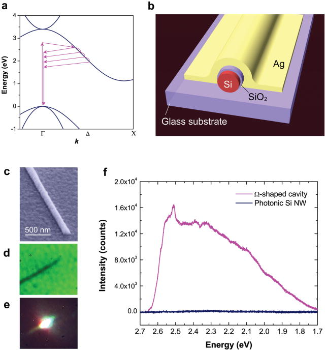
Due to limitations in device speed and performance of silicon-based electronics, silicon optoelectronics has been extensively studied to achieve ultrafast optical-data processing. However, the biggest challenge has been to develop an efficient silicon-based light source since indirect band-gap of silicon gives rise to extremely low emission efficiency. Although light emission in quantum-confined silicon at sub-10 nm lengthscales has been demonstrated, there are difficulties in integrating quantum structures with conventional electronics. It is desirable to develop new concepts to obtain emission from silicon at lengthscales compatible with current electronic devices (20-100 nm), which therefore do not utilize quantum-confinement effects. Here, we demonstrate an entirely new method to achieve bright visible light emission in "bulk-sized" silicon coupled with plasmon nanocavities from non-thermalized carrier recombination. Highly enhanced emission quantum efficiency (>1%) in plasmonic silicon, along with its size compatibility with present silicon electronics, provides new avenues for developing monolithically integrated light-sources on conventional microchips.
由于硅基电子器件在速度和性能方面存在局限性,硅光电子学已被广泛研究以实现超快速光数据处理。然而,最大的挑战一直是开发一种高效的硅基光源,因为硅的间接带隙导致极低的发射效率。尽管已证明在亚10纳米长度尺度的量子限制硅中存在光发射,但将量子结构与传统电子器件集成存在困难。期望开发新的概念,以在与当前电子器件兼容的长度尺度(20 - 100纳米)下从硅中获得发射,因此不利用量子限制效应。在此,我们展示了一种全新的方法,通过非热载流子复合在“块状”硅与等离子体纳米腔耦合中实现明亮的可见光发射。等离子体硅中高度增强的发射量子效率(>1%),以及其与当前硅电子器件的尺寸兼容性,为在传统微芯片上开发单片集成光源提供了新途径。