Department of Energy Conversion and Storage, Technical University of Denmark, Frederiksborgvej 399, DK-4000, Roskilde, Denmark.
ICFO - The Institute of Photonic Sciences, The Barcelona Institute of Science and Technology, 08860, Castelldefels (Barcelona), Spain.
Sci Rep. 2017 Jun 19;7(1):3787. doi: 10.1038/s41598-017-03891-7.
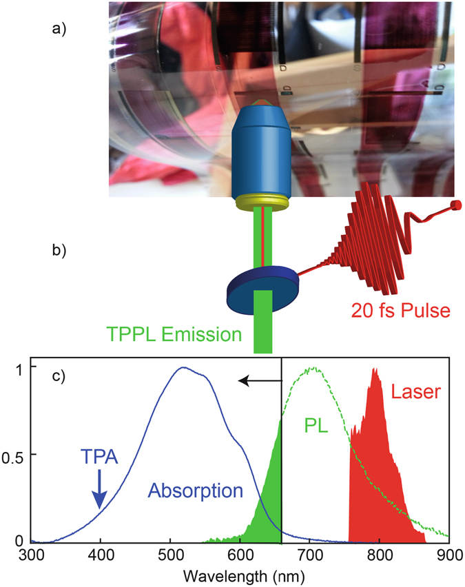
Printed electronics is emerging as a new, large scale and cost effective technology that will be disruptive in fields such as energy harvesting, consumer electronics and medical sensors. The performance of printed electronic devices relies principally on the carrier mobility and molecular packing of the polymer semiconductor material. Unfortunately, the analysis of such materials is generally performed with destructive techniques, which are hard to make compatible with in situ measurements, and pose a great obstacle for the mass production of printed electronics devices. A rapid, in situ, non-destructive and low-cost testing method is needed. In this study, we demonstrate that nonlinear optical microscopy is a promising technique to achieve this goal. Using ultrashort laser pulses we stimulate two-photon absorption in a roll coated polymer semiconductor and map the resulting two-photon induced photoluminescence and second harmonic response. We show that, in our experimental conditions, it is possible to relate the total amount of photoluminescence detected to important material properties such as the charge carrier density and the molecular packing of the printed polymer material, all with a spatial resolution of 400 nm. Importantly, this technique can be extended to the real time mapping of the polymer semiconductor film, even during the printing process, in which the high printing speed poses the need for equally high acquisition rates.
印刷电子技术作为一种新兴的、大规模且具有成本效益的技术正在能源收集、消费电子和医疗传感器等领域产生颠覆性影响。印刷电子设备的性能主要依赖于聚合物半导体材料的载流子迁移率和分子堆积。不幸的是,此类材料的分析通常采用破坏性技术,这些技术难以与原位测量兼容,这对印刷电子产品的大规模生产构成了巨大障碍。因此,需要一种快速、原位、无损且低成本的测试方法。在这项研究中,我们证明了非线性光学显微镜是实现这一目标的一种很有前途的技术。我们使用超短激光脉冲在滚涂聚合物半导体中激发双光子吸收,并绘制由此产生的双光子诱导光致发光和二次谐波响应。我们表明,在我们的实验条件下,有可能将检测到的总光致发光量与重要的材料特性相关联,例如电荷载流子密度和印刷聚合物材料的分子堆积,所有这些都具有 400nm 的空间分辨率。重要的是,该技术可以扩展到聚合物半导体薄膜的实时映射,即使在打印过程中,高打印速度也需要同样高的采集速率。