Department of Physics and Astronomy, University of Southampton, Southampton, SO17 1BJ, UK.
Center for Nanoscale Science and Technology, National Institute of Standards and Technology, Gaithersburg, MD, 20899, USA.
Sci Rep. 2017 Jul 24;7(1):6205. doi: 10.1038/s41598-017-06566-5.
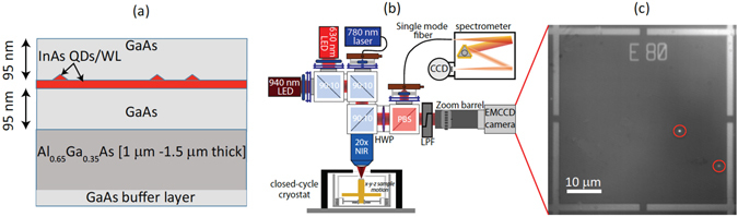
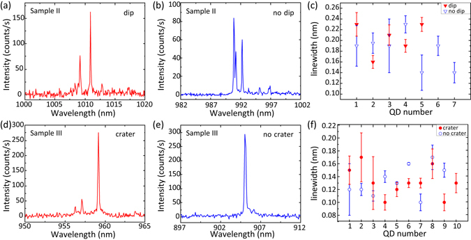
We report on a combined photoluminescence imaging and atomic force microscopy study of single, isolated self-assembled InAs quantum dots. The motivation of this work is to determine an approach that allows to assess single quantum dots as candidates for quantum nanophotonic devices. By combining optical and scanning probe characterization techniques, we find that single quantum dots often appear in the vicinity of comparatively large topographic features. Despite this, the quantum dots generally do not exhibit significant differences in their non-resonantly pumped emission spectra in comparison to quantum dots appearing in defect-free regions, and this behavior is observed across multiple wafers produced in different growth chambers. Such large surface features are nevertheless a detriment to applications in which single quantum dots are embedded within nanofabricated photonic devices: they are likely to cause large spectral shifts in the wavelength of cavity modes designed to resonantly enhance the quantum dot emission, thereby resulting in a nominally perfectly-fabricated single quantum dot device failing to behave in accordance with design. We anticipate that the approach of screening quantum dots not only based on their optical properties, but also their surrounding surface topographies, will be necessary to improve the yield of single quantum dot nanophotonic devices.
我们报告了一项关于单个孤立自组装 InAs 量子点的光致发光成像和原子力显微镜研究。这项工作的动机是确定一种方法,允许评估单个量子点作为量子纳米光子器件的候选者。通过结合光学和扫描探针表征技术,我们发现单个量子点通常出现在相对较大的形貌特征附近。尽管如此,与出现在无缺陷区域的量子点相比,单个量子点的非共振泵浦发射光谱通常没有明显差异,这种行为在不同生长室中制造的多个晶圆上都观察到。然而,这种大的表面特征对于将单个量子点嵌入纳米制造光子器件的应用来说是不利的:它们很可能导致设计用于共振增强量子点发射的腔模的波长发生大的光谱位移,从而导致名义上完美制造的单个量子点器件的行为不符合设计要求。我们预计,筛选量子点不仅要基于它们的光学性质,还要基于它们周围的表面形貌,这对于提高单个量子点纳米光子器件的产量是必要的。