Department of Mechanical Engineering, the Texas Center for Superconductivity, and Advanced Manufacturing Institute, University of Houston, Houston, TX, 77204, USA.
Applied Superconductivity Center, National High Magnet Field Laboratory, Florida State University, Tallahassee, FL, 32310, USA.
Sci Rep. 2017 Jul 31;7(1):6853. doi: 10.1038/s41598-017-06881-x.
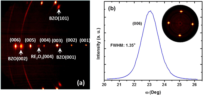
A main challenge that significantly impedes REBaCuO (RE = rare earth) coated conductor applications is the low engineering critical current density J because of the low superconductor fill factor in a complicated layered structure that is crucial for REBaCuO to carry supercurrent. Recently, we have successfully achieved engineering critical current density beyond 2.0 kA/mm at 4.2 K and 16 T, by growing thick REBaCuO layer, from ∼1.0 μm up to ∼3.2 μm, as well as controlling the pinning microstructure. Such high engineering critical current density, the highest value ever observed so far, establishes the essential role of REBaCuO coated conductors for very high field magnet applications. We attribute such excellent performance to the dense c-axis self-assembled BaZrO nanorods, the elimination of large misoriented grains, and the suppression of big second phase particles in this ~3.2 μm thick REBaCuO film.
主要挑战是,由于复杂层状结构中超导材料填充因子低,REBaCuO(RE=稀土)涂层导体的应用受到限制,而这对于超导电流的传输至关重要。最近,我们通过生长厚的 REBaCuO 层(从约 1.0μm 到约 3.2μm)并控制钉扎微结构,成功实现了在 4.2K 和 16T 下超过 2.0kA/mm 的工程临界电流密度,这是迄今为止观察到的最高值。如此高的工程临界电流密度确立了 REBaCuO 涂层导体在超高场磁体应用中的重要作用。我们将这种优异的性能归因于致密的 c 轴自组装 BaZrO 纳米棒、消除了大的取向差晶粒以及抑制了厚约 3.2μm 的 REBaCuO 薄膜中的大第二相粒子。