• 文献检索
  • 文档翻译
  • 深度研究
  • 学术资讯
  • Suppr Zotero 插件Zotero 插件
  • 邀请有礼
  • 套餐&价格
  • 历史记录
应用&插件
Suppr Zotero 插件Zotero 插件浏览器插件Mac 客户端Windows 客户端微信小程序
定价
高级版会员购买积分包购买API积分包
服务
文献检索文档翻译深度研究API 文档MCP 服务
关于我们
关于 Suppr公司介绍联系我们用户协议隐私条款
关注我们

Suppr 超能文献

核心技术专利:CN118964589B侵权必究
粤ICP备2023148730 号-1Suppr @ 2026

文献检索

告别复杂PubMed语法,用中文像聊天一样搜索,搜遍4000万医学文献。AI智能推荐,让科研检索更轻松。

立即免费搜索

文件翻译

保留排版,准确专业,支持PDF/Word/PPT等文件格式,支持 12+语言互译。

免费翻译文档

深度研究

AI帮你快速写综述,25分钟生成高质量综述,智能提取关键信息,辅助科研写作。

立即免费体验

广泛的纳米级化学对Cu(In, Ga)Se晶界处能带结构的影响。

Impact of Wide-Ranging Nanoscale Chemistry on Band Structure at Cu(In, Ga)Se Grain Boundaries.

作者信息

Stokes Adam, Al-Jassim Mowafak, Diercks David, Clarke Amy, Gorman Brian

机构信息

Colorado School of Mines, Material Science, Golden, CO, USA.

National Renewable Energy Laboratory, National Center for Photovoltaics, Golden, CO, USA.

出版信息

Sci Rep. 2017 Oct 26;7(1):14163. doi: 10.1038/s41598-017-14215-0.

DOI:10.1038/s41598-017-14215-0
PMID:29074885
原文链接:https://pmc.ncbi.nlm.nih.gov/articles/PMC5658345/
Abstract

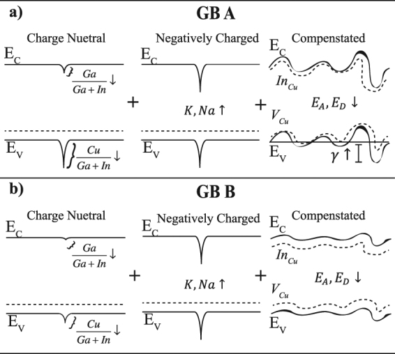
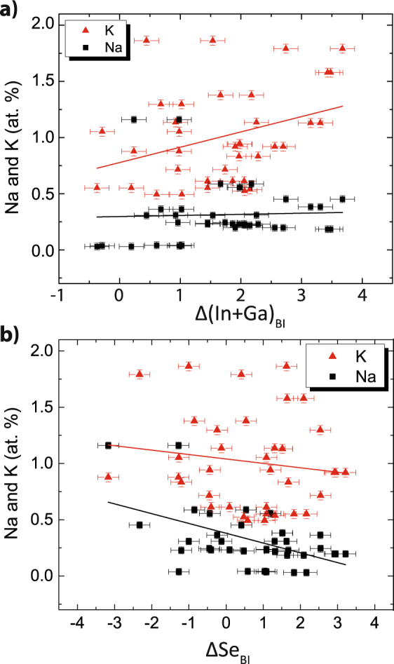
The relative chemistry from grain interiors to grain boundaries help explain why grain boundaries may be beneficial, detrimental or benign towards device performance. 3D Nanoscale chemical analysis extracted from atom probe tomography (APT) (10's of parts-per-million chemical sensitivity and sub-nanometer spatial resolution) of twenty grain boundaries in a high-efficiency Cu(In, Ga)Se solar cell shows the matrix and alkali concentrations are wide-ranging. The concentration profiles are then related to band structure which provide a unique insight into grain boundary electrical performance. Fluctuating Cu, In and Ga concentrations result in a wide distribution of potential barriers at the valence band maximum (VBM) (-10 to -160 meV) and the conduction band minimum (CBM) (-20 to -70 meV). Furthermore, Na and K segregation is not correlated to hampering donors, (In, Ga) and V, contrary to what has been previously reported. In addition, Na and K are predicted to be n-type dopants at grain boundaries. An overall band structure at grain boundaries is presented.

摘要

从晶粒内部到晶界的相关化学性质有助于解释为什么晶界对器件性能可能是有益的、有害的或无害的。从高效铜铟镓硒太阳能电池的20个晶界的原子探针断层扫描(APT)(百万分之几十的化学灵敏度和亚纳米空间分辨率)中提取的三维纳米级化学分析表明,基体和碱金属浓度范围很广。然后将浓度分布与能带结构相关联,这为深入了解晶界的电学性能提供了独特的视角。铜、铟和镓浓度的波动导致价带最大值(VBM)(-10至-160毫电子伏特)和导带最小值(CBM)(-20至-70毫电子伏特)处的势垒分布广泛。此外,与之前报道的情况相反,钠和钾的偏析与阻碍施主(铟、镓)和钒无关。此外,钠和钾预计在晶界处是n型掺杂剂。本文给出了晶界处的整体能带结构。

https://cdn.ncbi.nlm.nih.gov/pmc/blobs/2749/5658345/08a9432565e8/41598_2017_14215_Fig6_HTML.jpg
https://cdn.ncbi.nlm.nih.gov/pmc/blobs/2749/5658345/f3bc3223ac99/41598_2017_14215_Fig1_HTML.jpg
https://cdn.ncbi.nlm.nih.gov/pmc/blobs/2749/5658345/195a85ff2b11/41598_2017_14215_Fig2_HTML.jpg
https://cdn.ncbi.nlm.nih.gov/pmc/blobs/2749/5658345/8b7ee60b7b0d/41598_2017_14215_Fig3_HTML.jpg
https://cdn.ncbi.nlm.nih.gov/pmc/blobs/2749/5658345/c8986cdcf087/41598_2017_14215_Fig4_HTML.jpg
https://cdn.ncbi.nlm.nih.gov/pmc/blobs/2749/5658345/0e5d62cb6a69/41598_2017_14215_Fig5_HTML.jpg
https://cdn.ncbi.nlm.nih.gov/pmc/blobs/2749/5658345/08a9432565e8/41598_2017_14215_Fig6_HTML.jpg

相似文献

1
Impact of Wide-Ranging Nanoscale Chemistry on Band Structure at Cu(In, Ga)Se Grain Boundaries.广泛的纳米级化学对Cu(In, Ga)Se晶界处能带结构的影响。
Sci Rep. 2017 Oct 26;7(1):14163. doi: 10.1038/s41598-017-14215-0.
2
Evidence of Enhanced Carrier Collection in Cu(In,Ga)Se Grain Boundaries: Correlation with Microstructure.铜铟镓硒晶界中载流子收集增强的证据:与微观结构的相关性。
ACS Appl Mater Interfaces. 2018 May 2;10(17):14759-14766. doi: 10.1021/acsami.8b02328. Epub 2018 Apr 19.
3
Atom probe tomography studies on the Cu(In,ga)Se2 grain boundaries.关于Cu(In, Ga)Se₂晶界的原子探针断层扫描研究
J Vis Exp. 2013 Apr 22(74):50376. doi: 10.3791/50376.
4
Alkali Dispersion in (Ag,Cu)(In,Ga)Se Thin Film Solar Cells-Insight from Theory and Experiment.(银、铜)(铟、镓)硒薄膜太阳能电池中的碱分散——理论与实验的见解
ACS Appl Mater Interfaces. 2021 Feb 17;13(6):7188-7199. doi: 10.1021/acsami.0c20539. Epub 2021 Feb 3.
5
Atom-Scale Chemistry in Chalcopyrite-Based Photovoltaic Materials Visualized by Atom Probe Tomography.通过原子探针断层扫描可视化的基于黄铜矿的光伏材料中的原子尺度化学
ACS Appl Mater Interfaces. 2022 Nov 30;14(47):52825-52837. doi: 10.1021/acsami.2c14321. Epub 2022 Nov 8.
6
Large neutral barrier at grain boundaries in chalcopyrite thin films.黄铜矿薄膜晶界处的大型中性势垒。
Phys Rev Lett. 2010 May 14;104(19):196602. doi: 10.1103/PhysRevLett.104.196602.
7
Microstructural Characterization of Sulfurization Effects in Cu(In,Ga)Se2 Thin Film Solar Cells.Cu(In,Ga)Se2 薄膜太阳能电池中硫化效应的微观结构表征
Microsc Microanal. 2019 Apr;25(2):532-538. doi: 10.1017/S1431927619000151. Epub 2019 Mar 11.
8
Passivation of Deep-Level Defects by Cesium Fluoride Post-Deposition Treatment for Improved Device Performance of Cu(In,Ga)Se Solar Cells.氟化铯后沉积处理钝化深能级缺陷以提高铜铟镓硒太阳能电池器件性能。
ACS Appl Mater Interfaces. 2019 Oct 2;11(39):35653-35660. doi: 10.1021/acsami.9b08316. Epub 2019 Sep 17.
9
Complementary Characterization of Cu(In,Ga)Se₂ Thin-Film Photovoltaic Cells Using Secondary Ion Mass Spectrometry, Auger Electron Spectroscopy, and Atom Probe Tomography.使用二次离子质谱、俄歇电子能谱和原子探针断层扫描对 Cu(In,Ga)Se₂ 薄膜光伏电池进行补充表征。
J Nanosci Nanotechnol. 2018 May 1;18(5):3548-3556. doi: 10.1166/jnn.2018.14646.
10
Microscopic evidence for the modification of the electronic structure at grain boundaries of Cu(In(1-x),Ga(x))Se2 films.Cu(In(1-x),Ga(x))Se2 薄膜晶界电子结构修饰的微观证据。
Phys Rev Lett. 2012 Feb 17;108(7):076603. doi: 10.1103/PhysRevLett.108.076603. Epub 2012 Feb 14.

引用本文的文献

1
Cesium Modulation in Cu(In, Ga)(S, Se) Solar Cells: Comprehensive Analysis on Interface, Surface, and Grain Boundary.铜铟镓硒(Cu(In, Ga)(S, Se))太阳能电池中的铯调制:对界面、表面和晶界的综合分析
ACS Appl Mater Interfaces. 2024 Jun 26;16(25):32220-32231. doi: 10.1021/acsami.4c03680. Epub 2024 Jun 11.
2
Grain-boundary segregation of magnesium in doped cuprous oxide and impact on electrical transport properties.掺杂氧化亚铜中镁的晶界偏析及其对电输运性质的影响。
Sci Rep. 2021 Apr 8;11(1):7788. doi: 10.1038/s41598-021-86969-7.
3
Alkali Dispersion in (Ag,Cu)(In,Ga)Se Thin Film Solar Cells-Insight from Theory and Experiment.

本文引用的文献

1
Potassium Postdeposition Treatment-Induced Band Gap Widening at Cu(In,Ga)Se₂ Surfaces--Reason for Performance Leap?钾后沉积处理在 Cu(In,Ga)Se₂ 表面引起的带隙展宽——性能飞跃的原因?
ACS Appl Mater Interfaces. 2015 Dec 16;7(49):27414-20. doi: 10.1021/acsami.5b09231. Epub 2015 Dec 3.
2
The light and shade of perovskite solar cells.钙钛矿太阳能电池的明暗
Nat Mater. 2014 Sep;13(9):838-42. doi: 10.1038/nmat4065.
3
Potassium-induced surface modification of Cu(In,Ga)Se2 thin films for high-efficiency solar cells.钾诱导的铜铟镓硒薄膜的表面修饰用于高效太阳能电池。
(银、铜)(铟、镓)硒薄膜太阳能电池中的碱分散——理论与实验的见解
ACS Appl Mater Interfaces. 2021 Feb 17;13(6):7188-7199. doi: 10.1021/acsami.0c20539. Epub 2021 Feb 3.
4
Direct evidence for grain boundary passivation in Cu(In,Ga)Se solar cells through alkali-fluoride post-deposition treatments.通过碱金属氟化物沉积后处理实现Cu(In,Ga)Se太阳能电池中晶界钝化的直接证据。
Nat Commun. 2019 Sep 4;10(1):3980. doi: 10.1038/s41467-019-11996-y.
5
The Laplace Project: An integrated suite for preparing and transferring atom probe samples under cryogenic and UHV conditions.拉普拉斯项目:一套用于在低温和超高真空条件下准备和转移原子探针样品的集成套件。
PLoS One. 2018 Dec 21;13(12):e0209211. doi: 10.1371/journal.pone.0209211. eCollection 2018.
Nat Mater. 2013 Dec;12(12):1107-11. doi: 10.1038/nmat3789. Epub 2013 Nov 3.
4
Direct insight into grain boundary reconstruction in polycrystalline Cu(In,Ga)SE2 with atomic resolution.直接观察多晶 Cu(In,Ga)SE2 中的晶界重构,具有原子分辨率。
Phys Rev Lett. 2012 Feb 17;108(7):075502. doi: 10.1103/PhysRevLett.108.075502. Epub 2012 Feb 15.
5
Large neutral barrier at grain boundaries in chalcopyrite thin films.黄铜矿薄膜晶界处的大型中性势垒。
Phys Rev Lett. 2010 May 14;104(19):196602. doi: 10.1103/PhysRevLett.104.196602.
6
Electrically benign behavior of grain boundaries in polycrystalline CuInSe2 films.多晶CuInSe2薄膜中晶界的电学良性行为
Phys Rev Lett. 2007 Dec 7;99(23):235504. doi: 10.1103/PhysRevLett.99.235504.
7
In situ site-specific specimen preparation for atom probe tomography.用于原子探针断层扫描的原位特定位置样本制备
Ultramicroscopy. 2007 Feb-Mar;107(2-3):131-9. doi: 10.1016/j.ultramic.2006.06.008. Epub 2006 Jul 17.
8
Anomalous grain boundary physics in polycrystalline CuInSe2: the existence of a hole barrier.多晶CuInSe2中的异常晶界物理:空穴势垒的存在
Phys Rev Lett. 2003 Dec 31;91(26 Pt 1):266401. doi: 10.1103/PhysRevLett.91.266401. Epub 2003 Dec 24.