Stanford Synchrotron Radiation Lightsource, SLAC National Accelerator Laboratory , Menlo Park, California 94025, United States.
Department of Mechanical and Industrial Engineering, Norwegian University of Science and Technology , Trondheim 7491, Norway.
ACS Appl Mater Interfaces. 2017 Nov 15;9(45):39105-39109. doi: 10.1021/acsami.7b06728. Epub 2017 Nov 2.
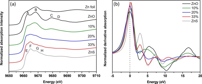
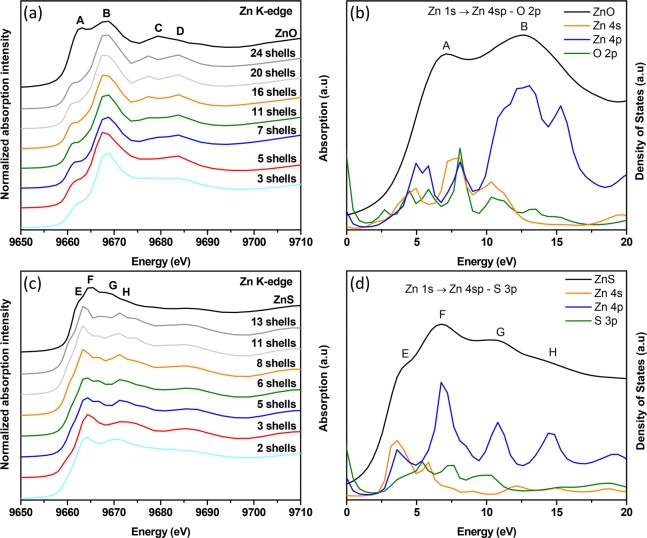
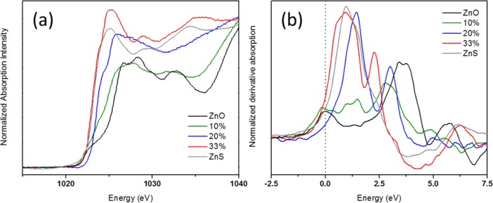
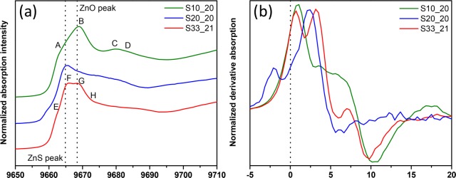
Zn(O,S) buffer layer electronic configuration is determined by its composition and thickness, tunable through atomic layer deposition. The Zn K and L-edges in the X-ray absorption near edge structure verify ionicity and covalency changes with S content. A high intensity shoulder in the Zn K-edge indicates strong Zn 4s hybridized states and a preferred c-axis orientation. 2-3 nm thick films with low S content show a subdued shoulder showing less contribution from Zn 4s hybridization. A lower energy shift with film thickness suggests a decreasing bandgap. Further, ZnSO forms at substrate interfaces, which may be detrimental for device performance.
Zn(O,S) 缓冲层的电子结构由其组成和厚度决定,可通过原子层沉积进行调节。X 射线吸收近边结构中的 Zn K 和 L 边验证了离子性和共价性随 S 含量的变化。Zn K 边的高强度肩表明存在强烈的 Zn 4s 杂化态和优先的 c 轴取向。具有低 S 含量的 2-3nm 厚薄膜显示出较不明显的肩,表明 Zn 4s 杂化的贡献较小。随着薄膜厚度的增加,能量位移降低表明带隙减小。此外,ZnSO 在衬底界面处形成,这可能对器件性能有害。