• 文献检索
  • 文档翻译
  • 深度研究
  • 学术资讯
  • Suppr Zotero 插件Zotero 插件
  • 邀请有礼
  • 套餐&价格
  • 历史记录
应用&插件
Suppr Zotero 插件Zotero 插件浏览器插件Mac 客户端Windows 客户端微信小程序
定价
高级版会员购买积分包购买API积分包
服务
文献检索文档翻译深度研究API 文档MCP 服务
关于我们
关于 Suppr公司介绍联系我们用户协议隐私条款
关注我们

Suppr 超能文献

核心技术专利:CN118964589B侵权必究
粤ICP备2023148730 号-1Suppr @ 2026

文献检索

告别复杂PubMed语法,用中文像聊天一样搜索,搜遍4000万医学文献。AI智能推荐,让科研检索更轻松。

立即免费搜索

文件翻译

保留排版,准确专业,支持PDF/Word/PPT等文件格式,支持 12+语言互译。

免费翻译文档

深度研究

AI帮你快速写综述,25分钟生成高质量综述,智能提取关键信息,辅助科研写作。

立即免费体验

殷钢薄膜上的四边形微孔阵列加工:湿法蚀刻与电化学熔合加工

Quadrilateral Micro-Hole Array Machining on Invar Thin Film: Wet Etching and Electrochemical Fusion Machining.

作者信息

Choi Woong-Kirl, Kim Seong-Hyun, Choi Seung-Geon, Lee Eun-Sang

机构信息

Department of Mechanical Engineering, Inha University, Incheon 402-751, Korea.

出版信息

Materials (Basel). 2018 Jan 19;11(1):160. doi: 10.3390/ma11010160.

DOI:10.3390/ma11010160
PMID:29351235
原文链接:https://pmc.ncbi.nlm.nih.gov/articles/PMC5793658/
Abstract

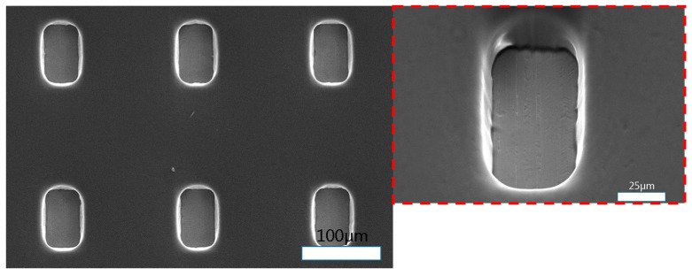
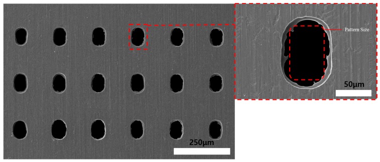
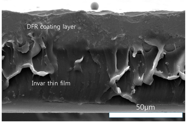
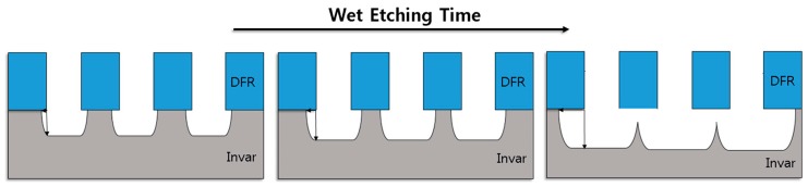
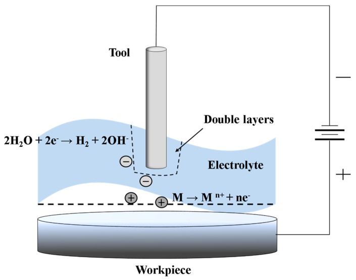
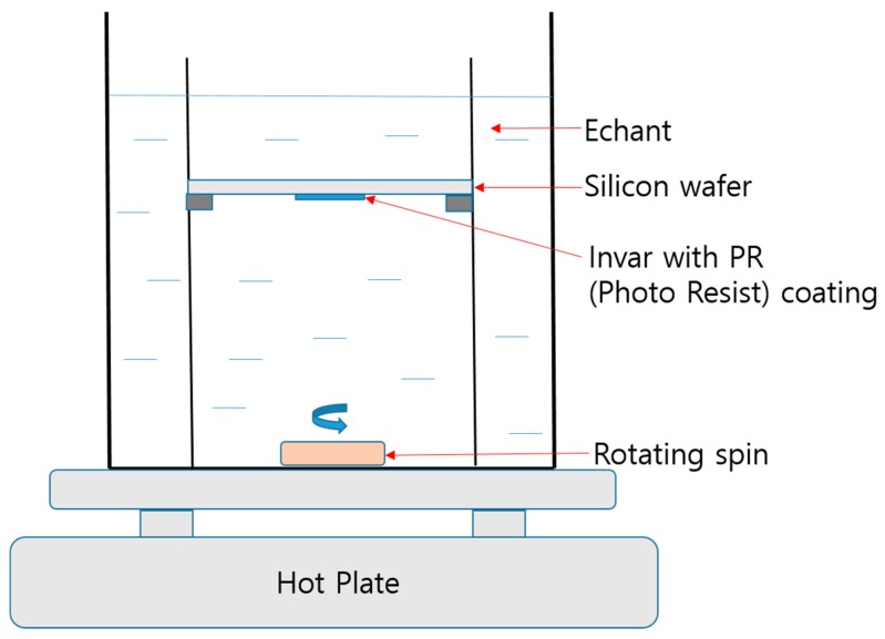
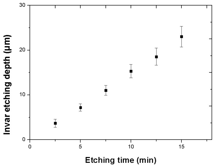
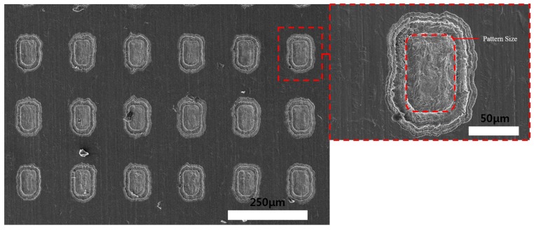
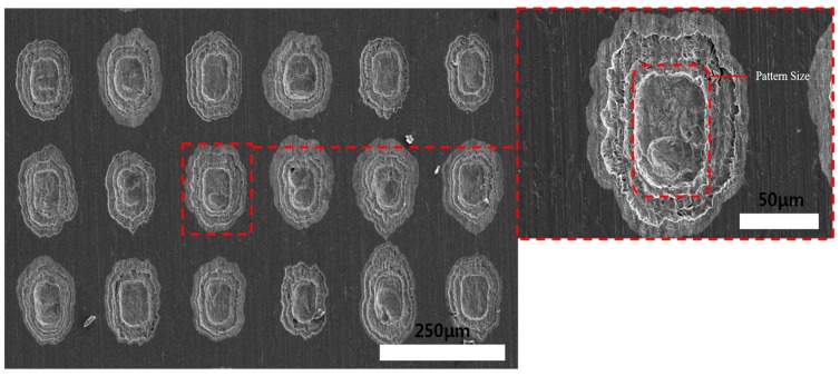
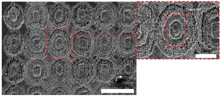
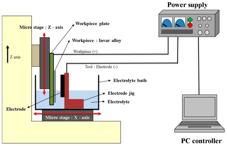
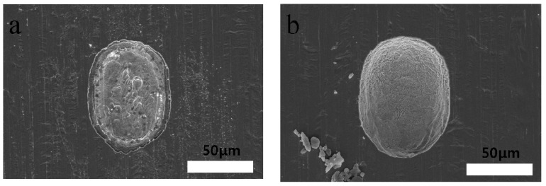
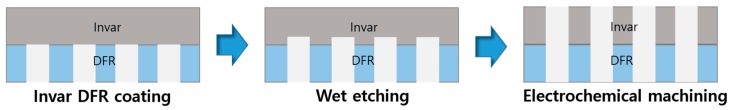
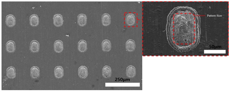
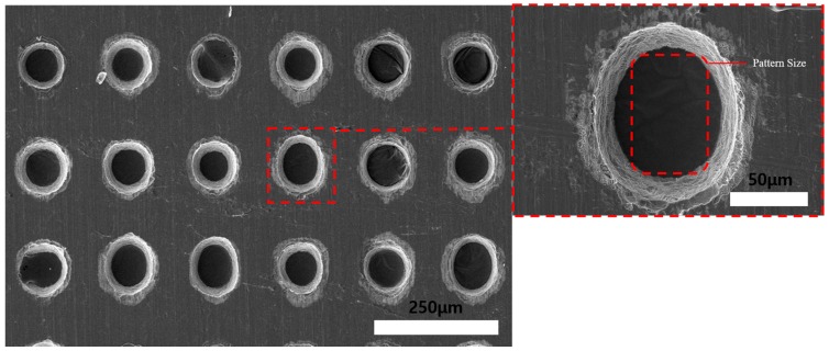
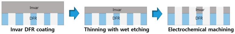
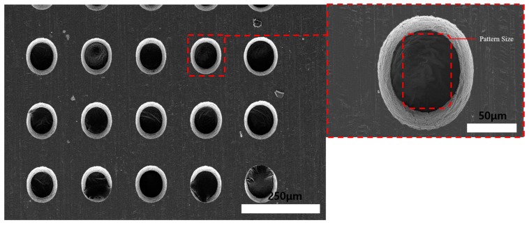
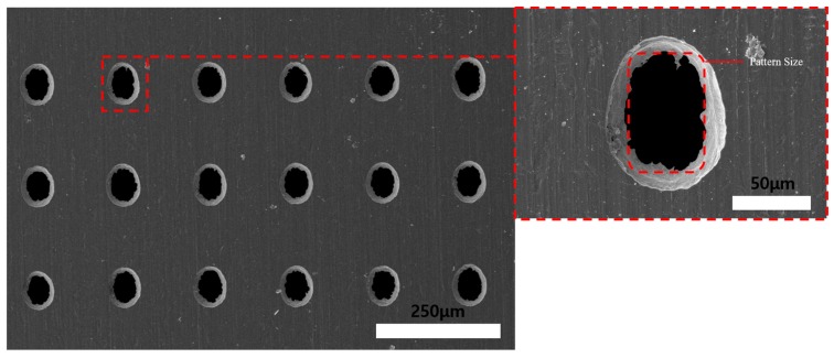
Ultra-precision products which contain a micro-hole array have recently shown remarkable demand growth in many fields, especially in the semiconductor and display industries. Photoresist etching and electrochemical machining are widely known as precision methods for machining micro-holes with no residual stress and lower surface roughness on the fabricated products. The Invar shadow masks used for organic light-emitting diodes (OLEDs) contain numerous micro-holes and are currently machined by a photoresist etching method. However, this method has several problems, such as uncontrollable hole machining accuracy, non-etched areas, and overcutting. To solve these problems, a machining method that combines photoresist etching and electrochemical machining can be applied. In this study, negative photoresist with a quadrilateral hole array pattern was dry coated onto 30-µm-thick Invar thin film, and then exposure and development were carried out. After that, photoresist single-side wet etching and a fusion method of wet etching-electrochemical machining were used to machine micro-holes on the Invar. The hole machining geometry, surface quality, and overcutting characteristics of the methods were studied. Wet etching and electrochemical fusion machining can improve the accuracy and surface quality. The overcutting phenomenon can also be controlled by the fusion machining. Experimental results show that the proposed method is promising for the fabrication of Invar film shadow masks.

摘要

最近,包含微孔阵列的超精密产品在许多领域,尤其是半导体和显示行业,需求增长显著。光刻胶蚀刻和电化学加工作为加工微孔的精密方法广为人知,其加工出的产品无残余应力且表面粗糙度较低。用于有机发光二极管(OLED)的因瓦荫罩包含大量微孔,目前采用光刻胶蚀刻法进行加工。然而,这种方法存在一些问题,如孔加工精度不可控、存在未蚀刻区域以及过蚀刻现象。为了解决这些问题,可以应用一种将光刻胶蚀刻和电化学加工相结合的加工方法。在本研究中,将具有四边形孔阵列图案的负性光刻胶干涂覆在30μm厚的因瓦薄膜上,然后进行曝光和显影。之后,采用光刻胶单侧湿法蚀刻以及湿法蚀刻 - 电化学加工的融合方法在因瓦上加工微孔。研究了这些方法的孔加工几何形状、表面质量和过蚀刻特性。湿法蚀刻和电化学融合加工可以提高精度和表面质量。过蚀刻现象也可以通过融合加工来控制。实验结果表明,所提出的方法对于制造因瓦薄膜荫罩具有很大的前景。

https://cdn.ncbi.nlm.nih.gov/pmc/blobs/f021/5793658/b3a47c654877/materials-11-00160-g018.jpg
https://cdn.ncbi.nlm.nih.gov/pmc/blobs/f021/5793658/40d01a3b76c5/materials-11-00160-g001.jpg
https://cdn.ncbi.nlm.nih.gov/pmc/blobs/f021/5793658/0fb0f4953ccc/materials-11-00160-g002.jpg
https://cdn.ncbi.nlm.nih.gov/pmc/blobs/f021/5793658/d8dbfe81afe9/materials-11-00160-g003.jpg
https://cdn.ncbi.nlm.nih.gov/pmc/blobs/f021/5793658/d87ab15cde37/materials-11-00160-g004.jpg
https://cdn.ncbi.nlm.nih.gov/pmc/blobs/f021/5793658/bd9ba4e6424c/materials-11-00160-g005.jpg
https://cdn.ncbi.nlm.nih.gov/pmc/blobs/f021/5793658/94ba9e37b130/materials-11-00160-g006.jpg
https://cdn.ncbi.nlm.nih.gov/pmc/blobs/f021/5793658/528a91fb60b6/materials-11-00160-g007.jpg
https://cdn.ncbi.nlm.nih.gov/pmc/blobs/f021/5793658/c88b9b78f4cf/materials-11-00160-g008.jpg
https://cdn.ncbi.nlm.nih.gov/pmc/blobs/f021/5793658/a494f6ffc9f0/materials-11-00160-g009.jpg
https://cdn.ncbi.nlm.nih.gov/pmc/blobs/f021/5793658/577283487dcb/materials-11-00160-g010.jpg
https://cdn.ncbi.nlm.nih.gov/pmc/blobs/f021/5793658/f6689178c5df/materials-11-00160-g011.jpg
https://cdn.ncbi.nlm.nih.gov/pmc/blobs/f021/5793658/a774b7fd93e1/materials-11-00160-g012.jpg
https://cdn.ncbi.nlm.nih.gov/pmc/blobs/f021/5793658/68ca97cdad4f/materials-11-00160-g013.jpg
https://cdn.ncbi.nlm.nih.gov/pmc/blobs/f021/5793658/cc91a4ff20fd/materials-11-00160-g014.jpg
https://cdn.ncbi.nlm.nih.gov/pmc/blobs/f021/5793658/effa980715dc/materials-11-00160-g015.jpg
https://cdn.ncbi.nlm.nih.gov/pmc/blobs/f021/5793658/4351eb33969f/materials-11-00160-g016.jpg
https://cdn.ncbi.nlm.nih.gov/pmc/blobs/f021/5793658/e5ca3aa919b8/materials-11-00160-g017.jpg
https://cdn.ncbi.nlm.nih.gov/pmc/blobs/f021/5793658/b3a47c654877/materials-11-00160-g018.jpg

相似文献

1
Quadrilateral Micro-Hole Array Machining on Invar Thin Film: Wet Etching and Electrochemical Fusion Machining.殷钢薄膜上的四边形微孔阵列加工:湿法蚀刻与电化学熔合加工
Materials (Basel). 2018 Jan 19;11(1):160. doi: 10.3390/ma11010160.
2
Fabrication of porous emitters for ionic liquid ion source by wire electrical discharge machining combined with electrochemical etching.通过电火花线切割加工与电化学蚀刻相结合制备用于离子液体离子源的多孔发射器。
Rev Sci Instrum. 2019 Dec 1;90(12):123304. doi: 10.1063/1.5099512.
3
Characteristics for electrochemical machining with nanoscale voltage pulses.纳米级电压脉冲电化学加工的特性
J Nanosci Nanotechnol. 2009 Jun;9(6):3424-32. doi: 10.1166/jnn.2009.ns12.
4
Ultrasonic-assisted electrochemical drill-grinding of small holes with high-quality.高质量小孔的超声辅助电化学钻磨
J Adv Res. 2020 Feb 15;23:151-161. doi: 10.1016/j.jare.2020.02.010. eCollection 2020 May.
5
Simulation Analysis and Process Evaluation of Cooling Hole Forming Precision in Mask Assisted Electrochemical Machining Based on GH4169.基于GH4169的掩膜辅助电化学加工冷却孔成型精度的仿真分析与工艺评估
Materials (Basel). 2022 Mar 7;15(5):1973. doi: 10.3390/ma15051973.
6
Confined Chemical Etching for Electrochemical Machining with Nanoscale Accuracy.限制化学刻蚀实现纳米级精度的电化学加工。
Acc Chem Res. 2016 Nov 15;49(11):2596-2604. doi: 10.1021/acs.accounts.6b00336. Epub 2016 Sep 26.
7
Effect of Conductive Coatings on Micro-Electro-Discharge Machinability of Aluminum Nitride Ceramic Using On-Machine-Fabricated Microelectrodes.导电涂层对使用机上制造的微电极加工氮化铝陶瓷微放电加工性能的影响。
Materials (Basel). 2019 Oct 11;12(20):3316. doi: 10.3390/ma12203316.
8
Experimental Investigation on Rotating Electrochemical Etching of a Micro Spiral Cylindrical Electrode.微螺旋圆柱电极旋转电化学蚀刻的实验研究
Micromachines (Basel). 2019 Oct 16;10(10):704. doi: 10.3390/mi10100704.
9
Anisotropic multi-step etching for large-area fabrication of surface microstructures on stainless steel to control thermal radiation.用于在不锈钢上大面积制造表面微结构以控制热辐射的各向异性多步蚀刻。
Sci Technol Adv Mater. 2015 Mar 17;16(2):025001. doi: 10.1088/1468-6996/16/2/025001. eCollection 2015 Apr.
10
Developments, challenges and future trends in advanced sustainable machining technologies for preparing array micro-holes.用于制备阵列微孔的先进可持续加工技术的发展、挑战及未来趋势
Nanoscale. 2024 Nov 7;16(43):19938-19969. doi: 10.1039/d4nr02910k.

引用本文的文献

1
Fabrication of Taper Free Micro-Holes Utilizing a Combined Rotating Helical Electrode and Short Voltage Pulse by ECM.采用旋转螺旋电极与短电压脉冲相结合的电化学加工方法制造无锥度微孔
Micromachines (Basel). 2019 Jan 3;10(1):28. doi: 10.3390/mi10010028.