Owiti Edgar O, Yang Hanning, Liu Peng, Ominde Calvine F, Sun Xiudong
Institute of Modern Optics, Department of Physics, Harbin Institute of Technology, Xi da zhi Road, Harbin, 150001, China.
Key Laboratory of Micro-Nano Optoelectronic Information System of Ministry of Industry and Information Technology, Xi da zhi Road, Harbin, 150001, Germany.
Nanoscale Res Lett. 2018 Feb 3;13(1):38. doi: 10.1186/s11671-017-2413-1.
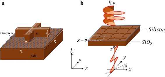
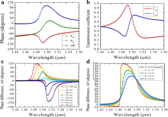
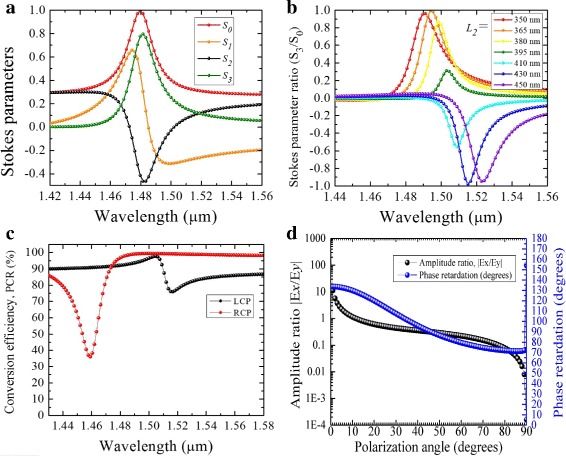
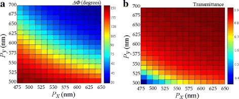
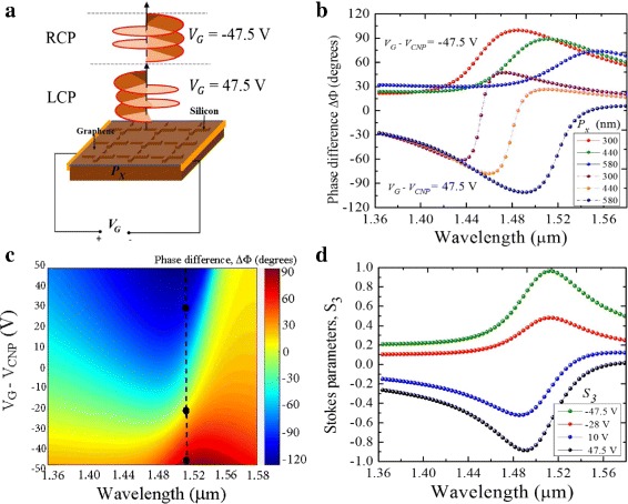
Previous studies on hybrid dielectric-graphene metasurfaces have been used to implement induced transparency devices, while exhibiting high Q-factors based on trapped magnetic resonances. Typically, the transparency windows are single wavelength and less appropriate for polarization conversion structures. In this work, a quarter-wave plate based on a hybrid silicon-graphene metasurface with controllable birefringence is numerically designed. The phenomena of trapped magnetic mode resonance and high Q-factors are modulated by inserting graphene between silicon and silica. This results in a broader transmission wavelength in comparison to the all-dielectric structure without graphene. The birefringence tunability is based on the dimensions of silicon and the Fermi energy of graphene. Consequently, a linear-to-circular polarization conversion is achieved at a high degree of 96%, in the near-infrared. Moreover, the polarization state of the scattered light is switchable between right and left hand circular polarizations, based on an external gate biasing voltage. Unlike in plasmonic metasurfaces, these achievements demonstrate an efficient structure that is free from radiative and ohmic losses. Furthermore, the ultrathin thickness and the compactness of the structure are demonstrated as key components in realizing integrable and CMOS compatible photonic sensors.
以往关于混合介质-石墨烯超表面的研究已被用于实现诱导透明器件,同时基于捕获的磁共振展现出高Q因子。通常,透明窗口是单一波长的,不太适合用于偏振转换结构。在这项工作中,数值设计了一种基于具有可控双折射的混合硅-石墨烯超表面的四分之一波片。通过在硅和二氧化硅之间插入石墨烯,调制了捕获磁模共振现象和高Q因子。与没有石墨烯的全介质结构相比,这导致了更宽的传输波长。双折射可调性基于硅的尺寸和石墨烯的费米能。因此,在近红外波段实现了高达96%的线偏振到圆偏振转换。此外,基于外部栅极偏置电压,散射光的偏振态可在右旋和左旋圆偏振之间切换。与等离子体超表面不同,这些成果展示了一种无辐射和欧姆损耗的高效结构。此外,超薄的厚度和结构的紧凑性被证明是实现可集成和CMOS兼容光子传感器的关键要素。