Lai Yiming, Mohamed Mohamed Sabry, Gao Boshen, Minkov Momchil, Boyd Robert W, Savona Vincenzo, Houdré Romuald, Badolato Antonio
Department of Physics University of Ottawa, Ottawa, Ontario, K1N 6N5, Canada.
Center for Nanoscale Science and Technology, National Institute of Standards and Technology, Gaithersburg, MD, 20899, USA.
Sci Rep. 2018 Oct 4;8(1):14811. doi: 10.1038/s41598-018-33090-x.
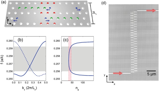
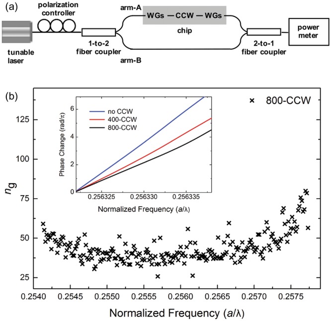
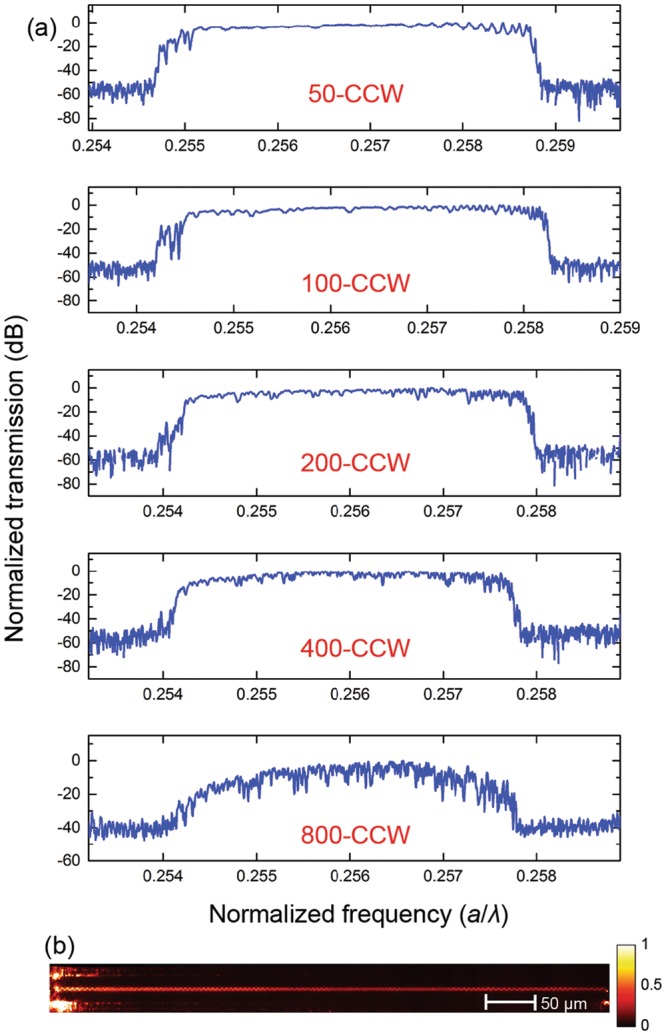
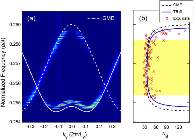
The ability of using integrated photonics to scale multiple optical components on a single monolithic chip offers key advantages to create miniature light-controlling chips. Numerous scaled optical components have been already demonstrated. However, present integrated photonic circuits are still rudimentary compared to the complexity of today's electronic circuits. Slow light propagation in nanostructured materials is a key component for realizing chip-integrated photonic devices controlling the relative phase of light and enhancing optical nonlinearities. We present an experimental record high group-index-bandwidth product (GBP) of 0.47 over a 17.7 nm bandwidth in genetically optimized coupled-cavity-waveguides (CCWs) formed by L3 photonic crystal cavities. Our structures were realized in silicon-on-insulator slabs integrating up to 800 coupled cavities, and characterized by transmission, Fourier-space imaging of mode dispersion, and Mach-Zehnder interferometry.
利用集成光子学在单个单片芯片上扩展多个光学组件的能力为创建微型光控芯片提供了关键优势。众多已缩放的光学组件已得到证明。然而,与当今电子电路的复杂性相比,目前的集成光子电路仍很初级。纳米结构材料中的慢光传播是实现控制光的相对相位并增强光学非线性的芯片集成光子器件的关键组成部分。我们展示了在由L3光子晶体腔形成的基因优化耦合腔波导(CCW)中,在17.7纳米带宽上实现了0.47的实验记录高群折射率带宽积(GBP)。我们的结构是在集成了多达800个耦合腔的绝缘体上硅平板中实现的,并通过传输、模式色散的傅里叶空间成像和马赫-曾德尔干涉测量进行了表征。