• 文献检索
  • 文档翻译
  • 深度研究
  • 学术资讯
  • Suppr Zotero 插件Zotero 插件
  • 邀请有礼
  • 套餐&价格
  • 历史记录
应用&插件
Suppr Zotero 插件Zotero 插件浏览器插件Mac 客户端Windows 客户端微信小程序
定价
高级版会员购买积分包购买API积分包
服务
文献检索文档翻译深度研究API 文档MCP 服务
关于我们
关于 Suppr公司介绍联系我们用户协议隐私条款
关注我们

Suppr 超能文献

核心技术专利:CN118964589B侵权必究
粤ICP备2023148730 号-1Suppr @ 2026

文献检索

告别复杂PubMed语法,用中文像聊天一样搜索,搜遍4000万医学文献。AI智能推荐,让科研检索更轻松。

立即免费搜索

文件翻译

保留排版,准确专业,支持PDF/Word/PPT等文件格式,支持 12+语言互译。

免费翻译文档

深度研究

AI帮你快速写综述,25分钟生成高质量综述,智能提取关键信息,辅助科研写作。

立即免费体验

有机场效应光学波导。

Organic field-effect optical waveguides.

机构信息

Beijing National Laboratory for Molecular Sciences, Key Laboratory of Organic Solids, Institute of Chemistry, Chinese Academy of Sciences, Beijing, 100190, China.

School of Chemistry and Chemical Engineering, University of the Chinese Academy of Sciences, Beijing, 100039, China.

出版信息

Nat Commun. 2018 Nov 15;9(1):4790. doi: 10.1038/s41467-018-07269-9.

DOI:10.1038/s41467-018-07269-9
PMID:30442889
原文链接:https://pmc.ncbi.nlm.nih.gov/articles/PMC6237772/
Abstract

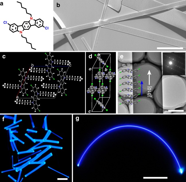
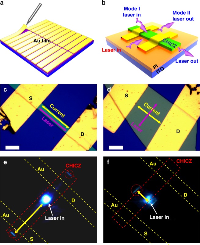
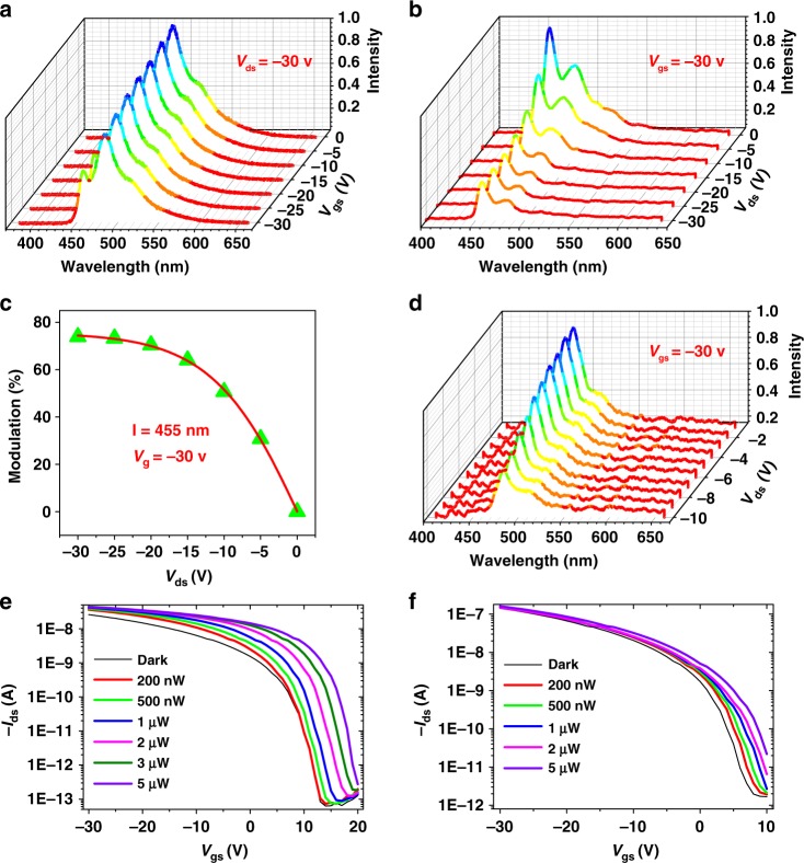
Integrating electronics and photonics is critically important for the realization of high-density and high-speed optoelectronic circuits. However, it remains challenging to achieve this target due to the difficulty of merging many different areas of science and technology. Here, we show an organic integrated optoelectronic device, namely, organic field-effect optical waveguide, integrating field-effect transistor and optical waveguide together. In such device, the propagation of optical waveguide in the active organic semiconductor can be tuned by the third terminal-the gate electrode of transistor, giving a controllable modulation depth as high as 70% and 50% in parallel and perpendicular directions of charge transport versus optical waveguide, respectively. Also, the optical waveguide with different directions can turn the field-effect of the device with the photodependence ratio up to 14800. The successful integration of active field-effect transistor with semiconductor waveguide modulator expands opportunities for creating scalable integration of electronics and photonics in a chip.

摘要

将电子学和光子学集成对于实现高密度和高速光电子电路至关重要。然而,由于融合许多不同科学和技术领域的难度,实现这一目标仍然具有挑战性。在这里,我们展示了一种有机集成光电设备,即有机场效应光波导,它将场效应晶体管和光波导集成在一起。在这种器件中,光学波导在有源有机半导体中的传播可以通过第三端——晶体管的栅电极来调节,在与光导垂直和平行的电荷输运方向上分别实现高达 70%和 50%的可控调制深度。此外,具有不同方向的光波导可以使器件的场效应随光依赖性比高达 14800。有源场效应晶体管与半导体波导调制器的成功集成为在芯片上实现电子学和光子学的可扩展集成创造了机会。

https://cdn.ncbi.nlm.nih.gov/pmc/blobs/42a4/6237772/1576904d44c4/41467_2018_7269_Fig4_HTML.jpg
https://cdn.ncbi.nlm.nih.gov/pmc/blobs/42a4/6237772/02aaf944ced4/41467_2018_7269_Fig1_HTML.jpg
https://cdn.ncbi.nlm.nih.gov/pmc/blobs/42a4/6237772/4f3cb44e7f5d/41467_2018_7269_Fig2_HTML.jpg
https://cdn.ncbi.nlm.nih.gov/pmc/blobs/42a4/6237772/209e5cb36e4a/41467_2018_7269_Fig3_HTML.jpg
https://cdn.ncbi.nlm.nih.gov/pmc/blobs/42a4/6237772/1576904d44c4/41467_2018_7269_Fig4_HTML.jpg

相似文献

1
Organic field-effect optical waveguides.有机场效应光学波导。
Nat Commun. 2018 Nov 15;9(1):4790. doi: 10.1038/s41467-018-07269-9.
2
Silicon-Waveguide-Integrated Carbon Nanotube Optoelectronic System on a Single Chip.单芯片上的硅波导集成碳纳米管光电系统
ACS Nano. 2020 Jun 23;14(6):7191-7199. doi: 10.1021/acsnano.0c02139. Epub 2020 May 26.
3
Polymer-Waveguide-Integrated 2D Semiconductor Heterostructures for Optical Communications.用于光通信的聚合物波导集成二维半导体异质结构
Nano Lett. 2023 Dec 13;23(23):11019-11025. doi: 10.1021/acs.nanolett.3c03317. Epub 2023 Nov 21.
4
Organic printed photonics: From microring lasers to integrated circuits.有机印刷光子学:从微环激光器到集成电路。
Sci Adv. 2015 Sep 18;1(8):e1500257. doi: 10.1126/sciadv.1500257. eCollection 2015 Sep.
5
Vertical Organic Field-Effect Transistors for Integrated Optoelectronic Applications.用于集成光电子应用的垂直有机场效应晶体管。
ACS Appl Mater Interfaces. 2016 Apr 27;8(16):10430-5. doi: 10.1021/acsami.6b00182. Epub 2016 Apr 15.
6
Asymmetric photon transport in organic semiconductor nanowires through electrically controlled exciton diffusion.通过电控激子扩散实现有机半导体纳米线中的非对称光子传输。
Sci Adv. 2018 Mar 16;4(3):eaap9861. doi: 10.1126/sciadv.aap9861. eCollection 2018 Mar.
7
2D Organic Photonics: An Asymmetric Optical Waveguide in Self-Assembled Halogen-Bonded Cocrystals.二维有机光子学:自组装卤键共晶体中的非对称光波导
Angew Chem Int Ed Engl. 2018 Aug 27;57(35):11300-11304. doi: 10.1002/anie.201806149. Epub 2018 Aug 17.
8
InGaAsP Mach-Zehnder interferometer optical modulator monolithically integrated with InGaAs driver MOSFET on a III-V CMOS photonics platform.在III-V族互补金属氧化物半导体光子学平台上与铟镓砷驱动金属氧化物半导体场效应晶体管单片集成的铟镓砷磷马赫-曾德尔干涉仪光调制器。
Opt Express. 2018 Feb 19;26(4):4842-4852. doi: 10.1364/OE.26.004842.
9
A high-speed silicon optical modulator based on a metal-oxide-semiconductor capacitor.一种基于金属氧化物半导体电容器的高速硅光调制器。
Nature. 2004 Feb 12;427(6975):615-8. doi: 10.1038/nature02310.
10
Control over multifunctionality in optoelectronic device based on organic phototransistor.基于有机光电晶体管的多功能性控制的光电子器件。
ACS Appl Mater Interfaces. 2010 Jun;2(6):1614-20. doi: 10.1021/am100127q.

引用本文的文献

1
High-Performance Phototransistor Based on a 2D Polybenzimidazole Polymer.基于二维聚苯并咪唑聚合物的高性能光电晶体管。
Adv Mater. 2025 Aug;37(33):e2505810. doi: 10.1002/adma.202505810. Epub 2025 Jun 1.
2
Flexible organic crystals with multi-stimuli-responsive CPL for broadband multicolor optical waveguides.具有多刺激响应圆偏振发光特性的柔性有机晶体用于宽带多色光波导
Chem Sci. 2024 Sep 27;15(42):17444-52. doi: 10.1039/d4sc05005c.
3
High-performance vertical field-effect organic photovoltaics.高性能垂直场效应有机光伏

本文引用的文献

1
Organic Semiconductor Single Crystals for Electronics and Photonics.有机半导体单晶用于电子学和光子学。
Adv Mater. 2018 Nov;30(44):e1801048. doi: 10.1002/adma.201801048. Epub 2018 Jul 23.
2
Asymmetric photon transport in organic semiconductor nanowires through electrically controlled exciton diffusion.通过电控激子扩散实现有机半导体纳米线中的非对称光子传输。
Sci Adv. 2018 Mar 16;4(3):eaap9861. doi: 10.1126/sciadv.aap9861. eCollection 2018 Mar.
3
Heterogeneous integration for on-chip quantum photonic circuits with single quantum dot devices.
Nat Commun. 2023 Mar 22;14(1):1579. doi: 10.1038/s41467-023-37174-9.
4
Identification of dyes and matrices for dye doped polymer waveguide emitters covering the visible spectrum.用于覆盖可见光谱的染料掺杂聚合物波导发射器的染料和基质的识别。
Sci Rep. 2022 Apr 12;12(1):6142. doi: 10.1038/s41598-022-10145-8.
用于集成单量子点器件的片上量子光子电路的异质集成
Nat Commun. 2017 Oct 12;8(1):889. doi: 10.1038/s41467-017-00987-6.
4
Organic Micro/Nanoscale Lasers.有机微/纳尺度激光器。
Acc Chem Res. 2016 Sep 20;49(9):1691-700. doi: 10.1021/acs.accounts.6b00209. Epub 2016 Aug 25.
5
Electrically controlled one-way photon flow in plasmonic nanostructures.等离子体纳米结构中的电控单向光流。
Nat Commun. 2014 Nov 6;5:5250. doi: 10.1038/ncomms6250.
6
From molecular design and materials construction to organic nanophotonic devices.从分子设计和材料构建到有机纳米光子器件。
Acc Chem Res. 2014 Dec 16;47(12):3448-58. doi: 10.1021/ar500192v. Epub 2014 Oct 24.
7
Optical wavelength filters based on photonic confinement in semiconductor nanowire homojunctions.基于半导体纳米线同质结中光子限制的光学波长滤波器。
Adv Mater. 2014 Jan;26(4):620-4, 663. doi: 10.1002/adma.201303482. Epub 2013 Dec 5.
8
Controlling the structures and photonic properties of organic nanomaterials by molecular design.通过分子设计控制有机纳米材料的结构和光子特性。
Angew Chem Int Ed Engl. 2013 Aug 12;52(33):8713-7. doi: 10.1002/anie.201302894. Epub 2013 Jul 5.
9
Photonic signal processing on electronic scales: electro-optical field-effect nanoplasmonic modulator.电子秤上的光子信号处理:电光场效应纳米等离子体调制器。
Phys Rev Lett. 2012 Aug 3;109(5):053901. doi: 10.1103/PhysRevLett.109.053901. Epub 2012 Jul 31.
10
Semiconducting π-conjugated systems in field-effect transistors: a material odyssey of organic electronics.场效应晶体管中的半导体π共轭体系:有机电子学的材料探索之旅。
Chem Rev. 2012 Apr 11;112(4):2208-67. doi: 10.1021/cr100380z. Epub 2011 Nov 23.