Salamin Y, Baeuerle B, Heni W, Abrecht F C, Josten A, Fedoryshyn Y, Haffner C, Bonjour R, Watanabe T, Burla M, Elder D L, Dalton L R, Leuthold J
ETH Zurich, Institute of Electromagnetic Fields (IEF), 8092 Zurich, Switzerland.
University of Washington, Department of Chemistry, Seattle, WA 98195-1700, USA.
Nat Photonics. 2018 Dec;12(12):749-753. doi: 10.1038/s41566-018-0281-6. Epub 2018 Oct 29.
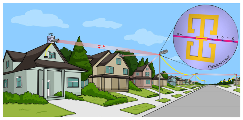
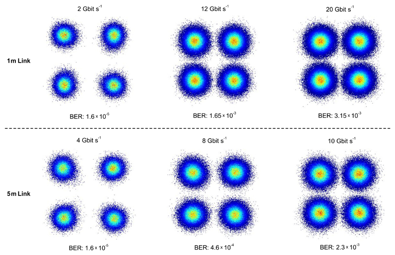
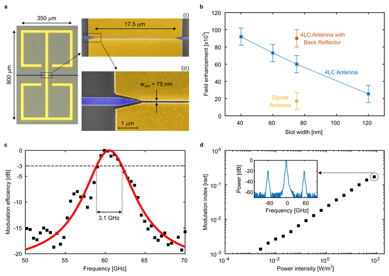
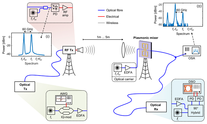
To cope with the high bandwidth requirements of wireless applications1, carrier frequencies are shifting towards the millimetre-wave and terahertz bands2-5. Conversely, data is normally transported to remote wireless antennas by optical fibres. Therefore, full transparency and flexibility to switch between optical and wireless domains would be desirable6,7. Here, we demonstrate for the first time a direct wireless-to-optical receiver in a transparent optical link. We successfully transmit 20 and 10 Gbit/s over wireless distances of 1 and 5 m at a carrier frequency of 60 GHz, respectively. Key to the breakthrough was a plasmonic mixer directly mapping the wireless information onto optical signals. The plasmonic scheme with its subwavelength feature and pronounced field confinement provides a built-in field enhancement of up to 90'000 over the incident field in an ultra-compact and CMOS compatible structure. The plasmonic mixer is not limited by electronic speed and thus compatible with future terahertz technologies.
为了满足无线应用对高带宽的需求1,载波频率正朝着毫米波和太赫兹频段转移2 - 5。相反,数据通常通过光纤传输到远程无线天线。因此,在光域和无线域之间实现完全透明和灵活切换将是理想的6,7。在此,我们首次展示了一种透明光链路中的直接无线到光接收器。我们分别在60 GHz载波频率下,在1米和5米的无线距离上成功传输了20 Gbit/s和10 Gbit/s的数据。这一突破的关键在于一种等离子体混频器,它能将无线信息直接映射到光信号上。这种具有亚波长特性和显著场限制的等离子体方案,在超紧凑且与CMOS兼容的结构中,能提供比入射场高达90000倍的内置场增强。该等离子体混频器不受电子速度限制,因此与未来的太赫兹技术兼容。