Mavuri Arunakumari, Mayes Andrew G, Alexander Matthew S
Engineering, Faculty of Science, University of East Anglia, Norwich NR4 7TJ, UK.
School of Chemistry, University of East Anglia, Norwich NR4 7TJ, UK.
Materials (Basel). 2019 Jul 15;12(14):2277. doi: 10.3390/ma12142277.
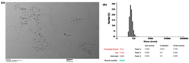
Printed electronics (PE) technology shows huge promise for the realisation of low-cost and flexible electronics, with the ability to pattern heat- or pressure-sensitive materials. In future developments of the PE market, the ability to produce highly conductive, high-resolution patterns using low-cost and roll-to-roll processes, such as inkjet printing, is a critical technology component for the fabrication of printed electronics and displays. Here, we demonstrate inkjet printing of polyacrylic acid (PAA) capped silver nanoparticle dispersions onto paper for high-conductivity electronic interconnects. We characterise the resulting print quality, feature geometry and electrical performance of inkjet patterned features and demonstrate the high-resolution printing, sub-100 micron feature size, of silver nanoparticle materials onto flexible paper substrate. Printed onto photo-paper, these materials then undergo chemically triggered sintering on exposure to chloride contained in the paper. We investigated the effect of substrate temperature on the properties of printed silver material from room temperature to 50 °C. At room temperature, the resistivity of single layer printed features, of average thickness of 500 nm and width 85 µm, was found to be 2.17 × 10 Ω·m or 13 times resistivity of bulk silver (RBS). The resistivity initially decreased with an increase in material thickness, when achieved by overprinting successive layers or by decreasing print pitch, and a resistivity of around 10 times RBS was observed after overprinting two times at pitch 75 µm and with single pass print pitch of between 60 and 80 µm, resulting in line thickness up to 920 nm. On further increases in thickness the resistivity increased and reached 27 times RBS at print pitch of 15 µm. On moderate heating of the substrate to 50 °C, more compact silver nanoparticle films were formed, reducing thickness to 200 nm from a single pass print, and lower material resistivity approaching five times RBS was achieved.
印刷电子(PE)技术在实现低成本和柔性电子方面展现出巨大潜力,它能够对热敏或压敏材料进行图案化处理。在PE市场的未来发展中,利用诸如喷墨打印等低成本且卷对卷工艺来生产高导电性、高分辨率图案的能力,是印刷电子产品和显示器制造的关键技术要素。在此,我们展示了将聚丙烯酸(PAA)包覆的银纳米颗粒分散体喷墨打印到纸张上以制备高导电性电子互连线路。我们对喷墨图案化特征的最终打印质量、特征几何形状和电气性能进行了表征,并展示了银纳米颗粒材料在柔性纸张基板上的高分辨率打印,特征尺寸小于100微米。这些材料打印在相纸上后,在接触纸张中所含的氯化物时会发生化学触发烧结。我们研究了从室温到50°C的基板温度对印刷银材料性能的影响。在室温下,平均厚度为500纳米、宽度为85微米的单层印刷特征的电阻率为2.17×10Ω·m,是块状银(RBS)电阻率的13倍。当通过叠加连续层或减小打印间距来增加材料厚度时,电阻率最初会降低,在75微米间距下叠加两次且单程打印间距在60至80微米之间(导致线路厚度达到920纳米)后,观察到电阻率约为RBS的10倍。随着厚度进一步增加,电阻率升高,在15微米打印间距时达到RBS的27倍。将基板适度加热至50°C时,会形成更致密的银纳米颗粒薄膜,单次打印的厚度从500纳米减小到200纳米,并且实现了更低的材料电阻率,接近RBS的5倍。