Matysiak Wiktor
Department of Engineering Materials and Biomaterials, Silesian University of Technology, Konarskiego 18A, 44-100, Gliwice, Poland.
Sci Rep. 2022 Mar 8;12(1):4046. doi: 10.1038/s41598-022-07830-z.
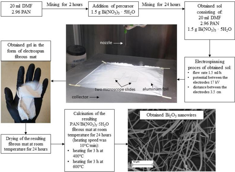
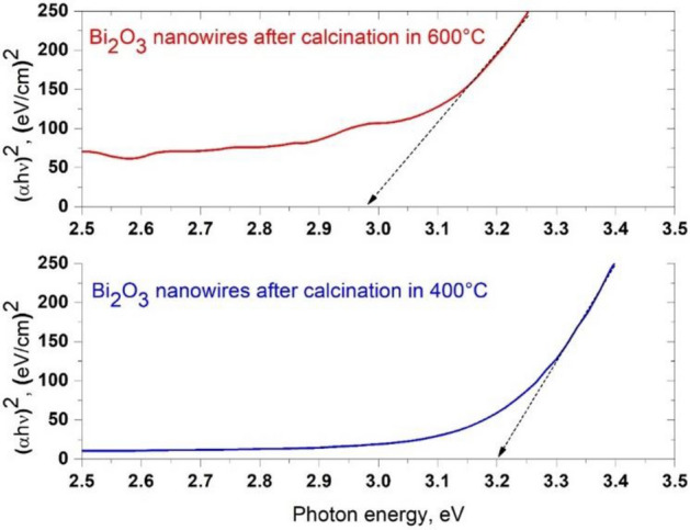
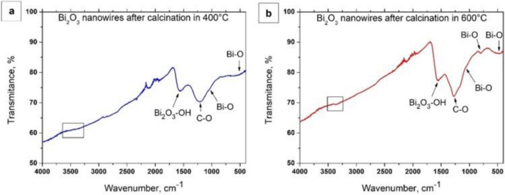
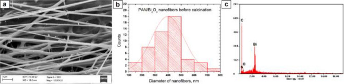
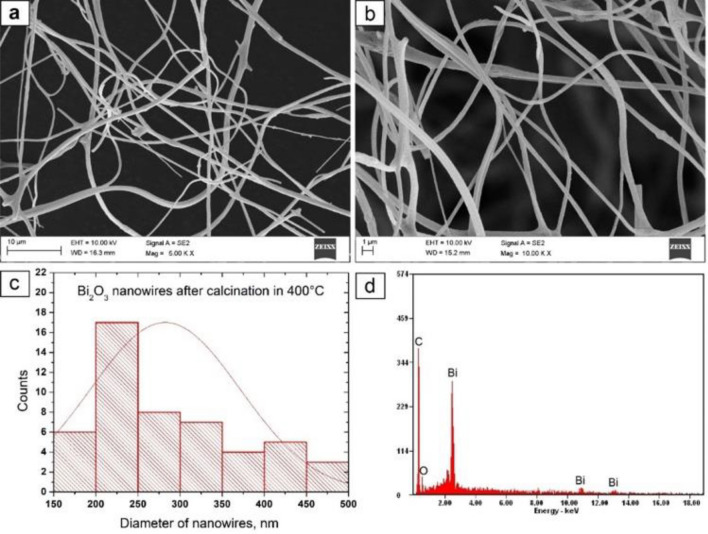
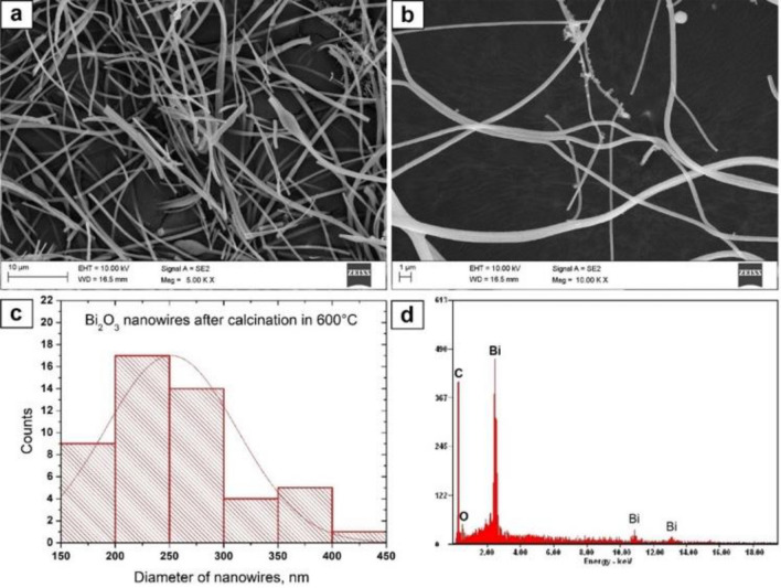
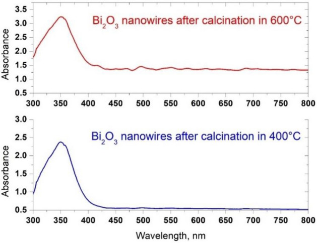
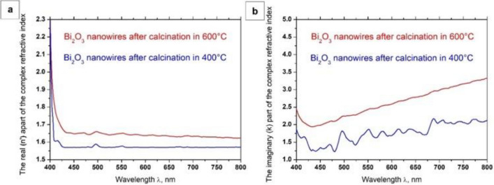
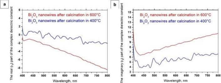
The aim of this study was to produce BiO nanowires using a combination of sol-gel process and electrospinning methods and a solution based on a 13% solution of polyacrylonitrile (PAN) in N,N-dimethylformamide (DMF) containing 1.5 g of bismuth (III) nitrate pentahydrate (Bi(NO)·5HO). The obtained fibrous composite mats were dried at room temperature for 24 h followed by the calcination process in air at two different temperatures of 400 °C and 600 °C. Analysis of the morphology of the fabricated BiO nanomaterials based on TEM images showed that the obtained ceramic structures could be classified as one-dimensional BiO nanostructures, with the sizes of the presented structures being 260 nm, 125 nm and 200 nm for diameter, and 5.5μm , 2 μm and 2.125 μm for length, respectively. Moreover, further analysis of the morphology of the obtained Bi2O3 nanostructures with the use of SEM showed that their diameters ranged from 150 to 500 nm when a calcination temperature of 400 °C was employed, while BiO nanowires with diameters ranging from 150 to 450 nm were obtained at 600 °C. To analyse the chemical composition and oscillatory transitions of atoms vibrating between the oscillatory levels in the molecules of the produced 1D nanostructures, and to determine the functional groups existing therein, EDX and FTIR were used. Transmission peaks in FTIR spectra recorded for wave numbers in the range of 400-4000 cm were due to the presence of vibrations in Bi-O bonds, which correspond to the structure of BiO. In addition, a detailed analysis of optical constants of one-dimensional BiO nanostructures fabricated using a combination of sol-gel process, electrospinning and calcination methods has been presented in this paper for the first time. Optical studies based on the recorded UV-Vis spectra showed that the obtained BiO nanowires were characterized by sharp absorption edges of radiation in the near-ultraviolet range, with sharp absorption edges falling at wavelengths of 400 nm, regardless of the applied temperature during the calcination process. The study of optical constants showed that the BiO nanostructures exhibited refractive indices of 2.62 and 2.53 at temperatures of 400 °C and 600 °C, respectively, while dielectric constants were 6.87 and 6.42, respectively. The final stage of the study was the determination of the width of energy gaps of the produced bismuth oxide nanostructures, which were found to be 3.19 and 2.97 eV, respectively. The presented results of morphology and optical properties of the obtained one-dimensional BiO semiconductor nanostructures indicate a potential possibility to apply this type of materials for the production of a new generation of dye-sensitized photovoltaic cells (DSSCs).
本研究的目的是结合溶胶 - 凝胶法和静电纺丝法制备Bi₂O₃纳米线,所使用的溶液是基于13%的聚丙烯腈(PAN)在N,N - 二甲基甲酰胺(DMF)中,并含有1.5 g五水硝酸铋(III)(Bi(NO₃)₃·5H₂O)。将得到的纤维复合垫在室温下干燥24小时,然后在空气中于400℃和600℃这两个不同温度下进行煅烧。基于透射电子显微镜(TEM)图像对所制备的Bi₂O₃纳米材料的形态分析表明,所获得的陶瓷结构可归类为一维Bi₂O₃纳米结构,所呈现结构的尺寸分别为直径260 nm、125 nm和200 nm,长度5.5μm、2μm和2.125μm。此外,使用扫描电子显微镜(SEM)对所获得的Bi₂O₃纳米结构的形态进行进一步分析表明,当煅烧温度为400℃时,其直径范围为150至500 nm,而在600℃时获得的Bi₂O₃纳米线直径范围为150至450 nm。为了分析所制备的一维纳米结构分子中原子在振荡能级之间振动时的化学成分和振荡跃迁,并确定其中存在的官能团,使用了能量色散X射线光谱(EDX)和傅里叶变换红外光谱(FTIR)。在400 - 4000 cm⁻¹波数范围内记录的FTIR光谱中的透射峰是由于Bi - O键中的振动存在,这与Bi₂O₃的结构相对应。此外,本文首次对采用溶胶 - 凝胶法、静电纺丝法和煅烧法相结合制备的一维Bi₂O₃纳米结构的光学常数进行了详细分析。基于记录的紫外 - 可见光谱的光学研究表明,所获得的Bi₂O₃纳米线的特征是在近紫外范围内具有尖锐的辐射吸收边缘,无论煅烧过程中所施加的温度如何,尖锐吸收边缘都落在400 nm波长处。光学常数研究表明,Bi₂O₃纳米结构在400℃和600℃温度下的折射率分别为2.62和2.53,而介电常数分别为6.87和6.42。研究的最后阶段是确定所制备的氧化铋纳米结构的能隙宽度,发现其分别为3.19和2.97 eV。所获得一维Bi₂O₃半导体纳米结构的形态和光学性质的呈现结果表明,这种类型的材料具有应用于新一代染料敏化光伏电池(DSSC)生产的潜在可能性。