Wu Cheng-Tse, Soliman Ahmed I A, Utsunomiya Toru, Ichii Takashi, Sugimura Hiroyuki
Department of Materials Science and Engineering, Graduate School of Engineering, Kyoto University Kyoto 606-8501 Japan
Chemistry Department, Faculty of Science, Assiut University Assiut 71516 Egypt.
RSC Adv. 2019 Oct 10;9(55):32313-32322. doi: 10.1039/c9ra07256j. eCollection 2019 Oct 7.
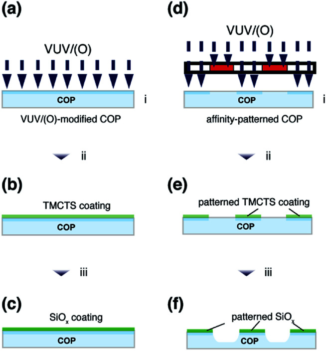
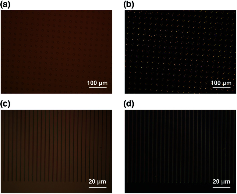
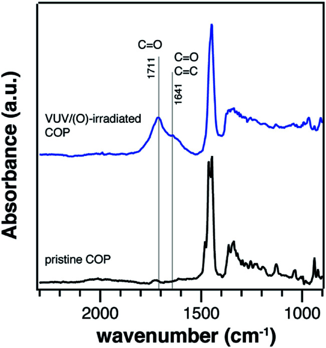
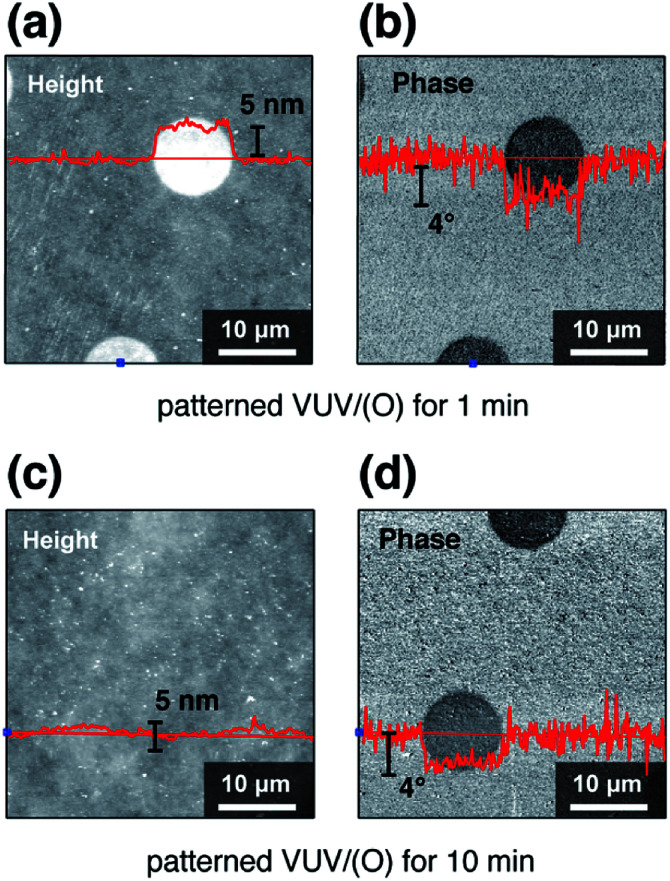
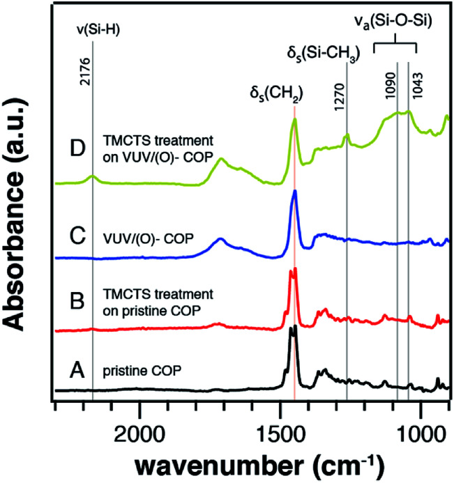
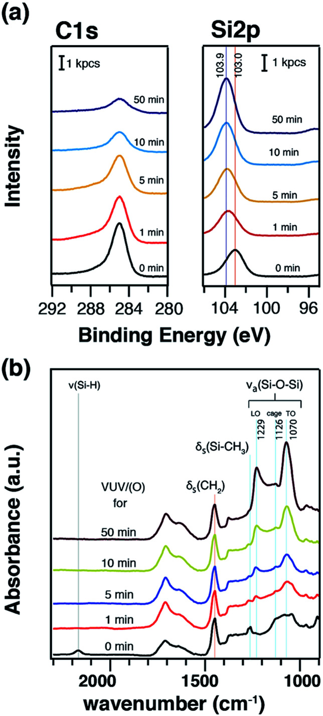
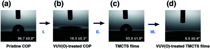
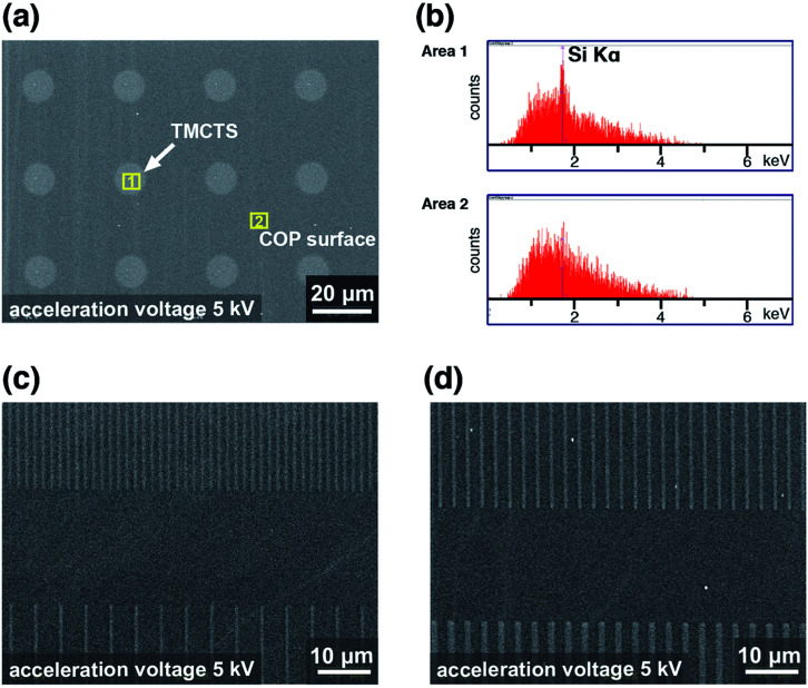
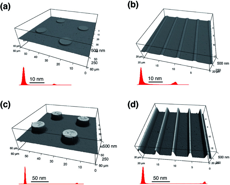
Formation of precise and high-resolution silica micropatterns on polymer substrates is of importance in surface structuring for flexible device fabrication of optics, microelectronic, and biotechnology. To achieve that, substrates modified with affinity-patterns serve as a strategy for site-selective deposition. In the present paper, vacuum ultraviolet (VUV) treatment is utilized to achieve spatially-controlled surface functionalization on a cyclo-olefin polymer (COP) substrate. An organosilane, 2,4,6,8-tetramethylcyclotetrasiloxane (TMCTS), preferentially deposits on the functionalized regions. Well-defined patterns of TMCTS are formed with a minimum feature of ∼500 nm. The secondary VUV/(O)-treatment converts TMCTS into SiO , meanwhile etches the bare COP surface, forming patterned SiO /COP microstructures with an average height of ∼150 nm. The resulting SiO patterns retain a good copy of TMCTS patterns, which are also consistent with the patterns of photomask used in polymer affinity-patterning. The high quality SiO patterns are of interests in microdevice fabrication, and the hydrophilicity contrast and adjustable heights reveal their potential application as a "stamp" for microcontact printing (μCP) techniques.
在聚合物基底上形成精确且高分辨率的二氧化硅微图案对于光学、微电子和生物技术等柔性器件制造的表面结构化至关重要。为实现这一目标,用亲和图案修饰的基底作为位点选择性沉积的一种策略。在本文中,利用真空紫外(VUV)处理在环烯烃聚合物(COP)基底上实现空间控制的表面功能化。一种有机硅烷,2,4,6,8 - 四甲基环四硅氧烷(TMCTS),优先沉积在功能化区域。形成了具有约500 nm最小特征尺寸的明确的TMCTS图案。二次VUV/(O)处理将TMCTS转化为SiO ,同时蚀刻裸露的COP表面,形成平均高度约为150 nm的图案化SiO /COP微结构。所得的SiO 图案很好地复制了TMCTS图案,这也与聚合物亲和图案化中使用的光掩模图案一致。高质量的SiO 图案在微器件制造中具有吸引力,并且亲水性对比和可调节的高度揭示了它们作为微接触印刷(μCP)技术的“印章”的潜在应用。