• 文献检索
  • 文档翻译
  • 深度研究
  • 学术资讯
  • Suppr Zotero 插件Zotero 插件
  • 邀请有礼
  • 套餐&价格
  • 历史记录
应用&插件
Suppr Zotero 插件Zotero 插件浏览器插件Mac 客户端Windows 客户端微信小程序
定价
高级版会员购买积分包购买API积分包
服务
文献检索文档翻译深度研究API 文档MCP 服务
关于我们
关于 Suppr公司介绍联系我们用户协议隐私条款
关注我们

Suppr 超能文献

核心技术专利:CN118964589B侵权必究
粤ICP备2023148730 号-1Suppr @ 2026

文献检索

告别复杂PubMed语法,用中文像聊天一样搜索,搜遍4000万医学文献。AI智能推荐,让科研检索更轻松。

立即免费搜索

文件翻译

保留排版,准确专业,支持PDF/Word/PPT等文件格式,支持 12+语言互译。

免费翻译文档

深度研究

AI帮你快速写综述,25分钟生成高质量综述,智能提取关键信息,辅助科研写作。

立即免费体验

使用线性回归分析评估多晶锗层中的受主缺陷。

Acceptor defects in polycrystalline Ge layers evaluated using linear regression analysis.

作者信息

Imajo Toshifumi, Ishiyama Takamitsu, Nozawa Koki, Suemasu Takashi, Toko Kaoru

机构信息

Institute of Applied Physics, University of Tsukuba, 1-1-1 Tennodai, Tsukuba, Ibaraki, 305-8573, Japan.

JSPS Research Fellow, 8 Ichiban-cho, Chiyoda-ku, Tokyo, 102-8472, Japan.

出版信息

Sci Rep. 2022 Sep 2;12(1):14941. doi: 10.1038/s41598-022-19221-5.

DOI:10.1038/s41598-022-19221-5
PMID:36056074
原文链接:https://pmc.ncbi.nlm.nih.gov/articles/PMC9440008/
Abstract

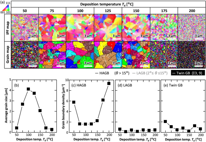
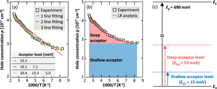
Polycrystalline Ge thin films have recently attracted renewed attention as a material for various electronic and optical devices. However, the difficulty in the Fermi level control of polycrystalline Ge films owing to their high density of defect-induced acceptors has limited their application in the aforementioned devices. Here, we experimentally estimated the origin of acceptor defects by significantly modulating the crystallinity and electrical properties of polycrystalline Ge layers and investigating their correlation. Our proposed linear regression analysis method, which is based on deriving the acceptor levels and their densities from the temperature dependence of the hole concentration, revealed the presence of two different acceptor levels. A systematic analysis of the effects of grain size and post annealing on the hole concentration suggests that deep acceptor levels (53-103 meV) could be attributed to dangling bonds located at grain boundaries, whereas shallow acceptor levels (< 15 meV) could be attributed to vacancies in grains. Thus, this study proposed a machine learning-based simulation method that can be widely applied in the analysis of physical properties, and can provide insights into the understanding and control of acceptor defects in polycrystalline Ge thin films.

摘要

多晶锗薄膜作为一种用于各种电子和光学器件的材料,最近重新引起了人们的关注。然而,由于多晶锗薄膜中缺陷诱导的受主密度高,其费米能级控制困难,限制了它们在上述器件中的应用。在此,我们通过显著调节多晶锗层的结晶度和电学性质并研究它们之间的相关性,从实验上估计了受主缺陷的起源。我们提出的线性回归分析方法基于从空穴浓度的温度依赖性推导出受主能级及其密度,揭示了存在两种不同的受主能级。对晶粒尺寸和退火后处理对空穴浓度影响的系统分析表明,深受主能级(53 - 103毫电子伏)可能归因于位于晶界处的悬空键,而浅受主能级(< 15毫电子伏)可能归因于晶粒中的空位。因此,本研究提出了一种基于机器学习的模拟方法,该方法可广泛应用于物理性质分析,并能为理解和控制多晶锗薄膜中的受主缺陷提供见解。

https://cdn.ncbi.nlm.nih.gov/pmc/blobs/e16c/9440008/ca56d2984ee3/41598_2022_19221_Fig5_HTML.jpg
https://cdn.ncbi.nlm.nih.gov/pmc/blobs/e16c/9440008/04ba08fc5280/41598_2022_19221_Fig1_HTML.jpg
https://cdn.ncbi.nlm.nih.gov/pmc/blobs/e16c/9440008/65a8ef5b5441/41598_2022_19221_Fig2_HTML.jpg
https://cdn.ncbi.nlm.nih.gov/pmc/blobs/e16c/9440008/fa8229b34150/41598_2022_19221_Fig3_HTML.jpg
https://cdn.ncbi.nlm.nih.gov/pmc/blobs/e16c/9440008/ebe3ba63b76c/41598_2022_19221_Fig4_HTML.jpg
https://cdn.ncbi.nlm.nih.gov/pmc/blobs/e16c/9440008/ca56d2984ee3/41598_2022_19221_Fig5_HTML.jpg

相似文献

1
Acceptor defects in polycrystalline Ge layers evaluated using linear regression analysis.使用线性回归分析评估多晶锗层中的受主缺陷。
Sci Rep. 2022 Sep 2;12(1):14941. doi: 10.1038/s41598-022-19221-5.
2
Strain-dependent grain boundary properties of n-type germanium layers.n型锗层的应变依赖性晶界特性
Sci Rep. 2024 Apr 3;14(1):7812. doi: 10.1038/s41598-024-56282-0.
3
Strain effects on polycrystalline germanium thin films.应变对多晶锗薄膜的影响。
Sci Rep. 2021 Apr 15;11(1):8333. doi: 10.1038/s41598-021-87616-x.
4
High-electron-mobility (370 cm/Vs) polycrystalline Ge on an insulator formed by As-doped solid-phase crystallization.通过砷掺杂固相结晶在绝缘体上形成的高电子迁移率(370 cm²/V·s)多晶锗。
Sci Rep. 2019 Nov 12;9(1):16558. doi: 10.1038/s41598-019-53084-7.
5
Improving carrier mobility of polycrystalline Ge by Sn doping.通过锡掺杂提高多晶锗的载流子迁移率。
Sci Rep. 2018 Oct 4;8(1):14832. doi: 10.1038/s41598-018-33161-z.
6
Imaging the Hydrogen Absorption Dynamics of Individual Grains in Polycrystalline Palladium Thin Films in 3D.三维成像研究多晶钯薄膜中单个晶粒的吸氢动力学。
ACS Nano. 2017 Nov 28;11(11):10945-10954. doi: 10.1021/acsnano.7b04735. Epub 2017 Oct 23.
7
Grain size dependent photoresponsivity in GaAs films formed on glass with Ge seed layers.在带有锗籽晶层的玻璃上形成的砷化镓薄膜中与晶粒尺寸相关的光响应性。
Sci Rep. 2021 May 12;11(1):10159. doi: 10.1038/s41598-021-89342-w.
8
Electrical and Structural Characteristics of Excimer Laser-Crystallized Polycrystalline SiGe Thin-Film Transistors.准分子激光结晶多晶SiGe薄膜晶体管的电学和结构特性
Materials (Basel). 2019 May 29;12(11):1739. doi: 10.3390/ma12111739.
9
Organic Cation Diffusion-Induced Heterogeneous Viscoelasticity in Organic-Inorganic Hybrid Perovskite Polycrystalline Films.有机阳离子扩散诱导的有机-无机杂化钙钛矿多晶薄膜中的非均匀粘弹性
ACS Appl Mater Interfaces. 2022 May 18;14(19):22582-22592. doi: 10.1021/acsami.2c01632. Epub 2022 May 9.
10
The hunt for the third acceptor in CuInSe and Cu(In,Ga)Se absorber layers.寻找铜铟硒和铜铟镓硒吸收层中的第三种受主。
J Phys Condens Matter. 2019 Oct 23;31(42):425702. doi: 10.1088/1361-648X/ab2e24. Epub 2019 Jul 1.

引用本文的文献

1
Strain-dependent grain boundary properties of n-type germanium layers.n型锗层的应变依赖性晶界特性
Sci Rep. 2024 Apr 3;14(1):7812. doi: 10.1038/s41598-024-56282-0.

本文引用的文献

1
Strain effects on polycrystalline germanium thin films.应变对多晶锗薄膜的影响。
Sci Rep. 2021 Apr 15;11(1):8333. doi: 10.1038/s41598-021-87616-x.
2
High-electron-mobility (370 cm/Vs) polycrystalline Ge on an insulator formed by As-doped solid-phase crystallization.通过砷掺杂固相结晶在绝缘体上形成的高电子迁移率(370 cm²/V·s)多晶锗。
Sci Rep. 2019 Nov 12;9(1):16558. doi: 10.1038/s41598-019-53084-7.
3
Improving carrier mobility of polycrystalline Ge by Sn doping.通过锡掺杂提高多晶锗的载流子迁移率。
Sci Rep. 2018 Oct 4;8(1):14832. doi: 10.1038/s41598-018-33161-z.
4
High-hole mobility polycrystalline Ge on an insulator formed by controlling precursor atomic density for solid-phase crystallization.通过控制前驱体原子密度进行固相结晶在绝缘体上形成的高空穴迁移率多晶锗。
Sci Rep. 2017 Dec 5;7(1):16981. doi: 10.1038/s41598-017-17273-6.
5
Novel Ge waveguide platform on Ge-on-insulator wafer for mid-infrared photonic integrated circuits.用于中红外光子集成电路的绝缘体上锗晶圆上的新型锗波导平台。
Opt Express. 2016 May 30;24(11):11855-64. doi: 10.1364/OE.24.011855.