Jiménez-Arévalo Nuria, Al Shuhaib Jinan H, Pacheco Rodrigo Bautista, Marchiani Dario, Saad Abdelnabi Mahmoud M, Frisenda Riccardo, Sbroscia Marco, Betti Maria Grazia, Mariani Carlo, Manzanares-Negro Yolanda, Navarro Cristina Gómez, Martínez-Galera Antonio J, Ares José Ramón, Ferrer Isabel J, Leardini Fabrice
Departamento de Física de Materiales, Universidad Autónoma de Madrid, 28049, Madrid, Spain.
Dipartimento di Física, Sapienza Università di Roma, 00185 Roma, Italy.
ACS Appl Mater Interfaces. 2023 Jul 19;15(28):33514-33524. doi: 10.1021/acsami.3c02192. Epub 2023 Jul 5.
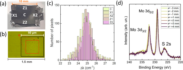
Tuning the electrocatalytic properties of MoS layers can be achieved through different paths, such as reducing their thickness, creating edges in the MoS flakes, and introducing S-vacancies. We combine these three approaches by growing MoS electrodes by using a special salt-assisted chemical vapor deposition (CVD) method. This procedure allows the growth of ultrathin MoS nanocrystals (1-3 layers thick and a few nanometers wide), as evidenced by atomic force microscopy and scanning tunneling microscopy. This morphology of the MoS layers at the nanoscale induces some specific features in the Raman and photoluminescence spectra compared to exfoliated or microcrystalline MoS layers. Moreover, the S-vacancy content in the layers can be tuned during CVD growth by using Ar/H mixtures as a carrier gas. Detailed optical microtransmittance and microreflectance spectroscopies, micro-Raman, and X-ray photoelectron spectroscopy measurements with sub-millimeter spatial resolution show that the obtained samples present an excellent homogeneity over areas in the cm range. The electrochemical and photoelectrochemical properties of these MoS layers were investigated using electrodes with relatively large areas (0.8 cm). The prepared MoS cathodes show outstanding Faradaic efficiencies as well as long-term stability in acidic solutions. In addition, we demonstrate that there is an optimal number of S-vacancies to improve the electrochemical and photoelectrochemical performances of MoS.
通过不同途径可以实现对MoS层电催化性能的调控,比如减小其厚度、在MoS薄片中制造边缘以及引入硫空位。我们通过使用一种特殊的盐辅助化学气相沉积(CVD)方法生长MoS电极,将这三种方法结合起来。如原子力显微镜和扫描隧道显微镜所证实的,该过程能够生长出超薄的MoS纳米晶体(1 - 3层厚且几纳米宽)。与剥离的或微晶的MoS层相比,这种纳米尺度的MoS层形态在拉曼光谱和光致发光光谱中呈现出一些特定特征。此外,在CVD生长过程中,可以通过使用Ar/H混合气体作为载气来调节层中的硫空位含量。具有亚毫米空间分辨率的详细光学微透射率和微反射率光谱、显微拉曼光谱以及X射线光电子能谱测量表明,所获得的样品在厘米范围内的区域具有出色的均匀性。使用面积相对较大(0.8平方厘米)的电极对这些MoS层的电化学和光电化学性质进行了研究。制备的MoS阴极在酸性溶液中表现出出色的法拉第效率以及长期稳定性。此外,我们证明存在一个最佳的硫空位数量,以改善MoS的电化学和光电化学性能。