Department of Telecommunications Engineering, School of Engineering, King Mongkut's Institute of Technology Ladkrabang, Bangkok 10520, Thailand.
Department of Microelectronics, Brno University of Technology, Technická 10, 616 00 Brno, Czech Republic.
Sensors (Basel). 2023 Jun 26;23(13):5945. doi: 10.3390/s23135945.
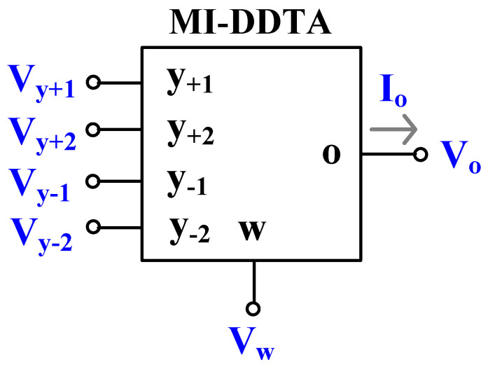
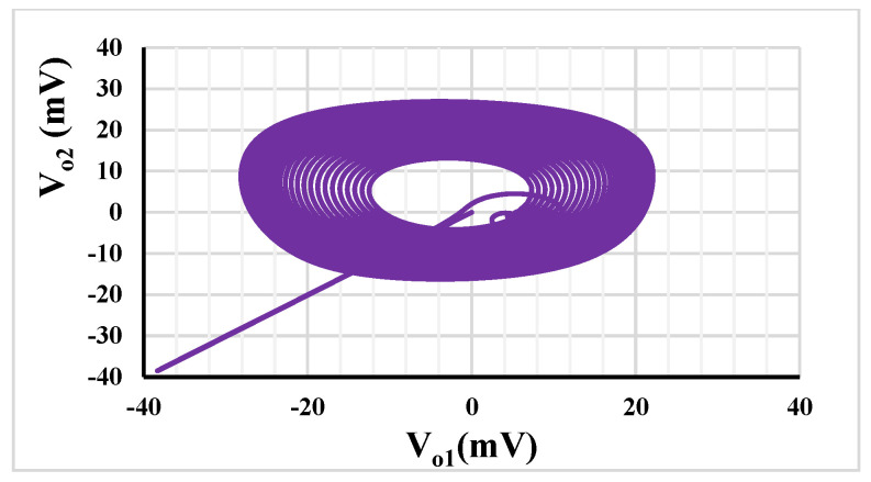
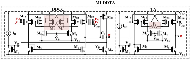
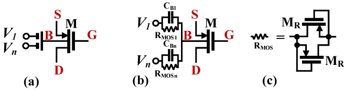
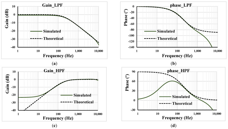
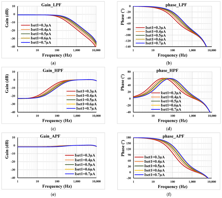
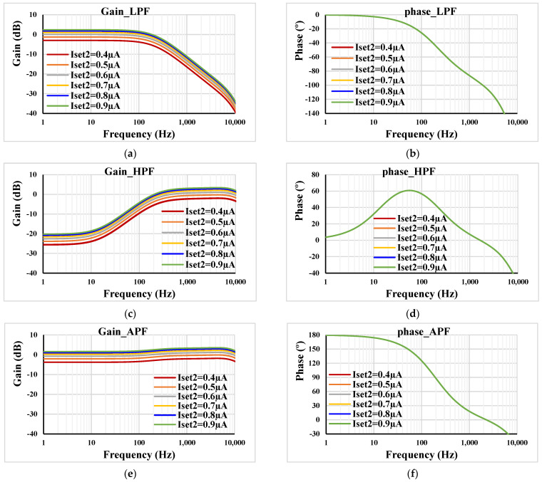
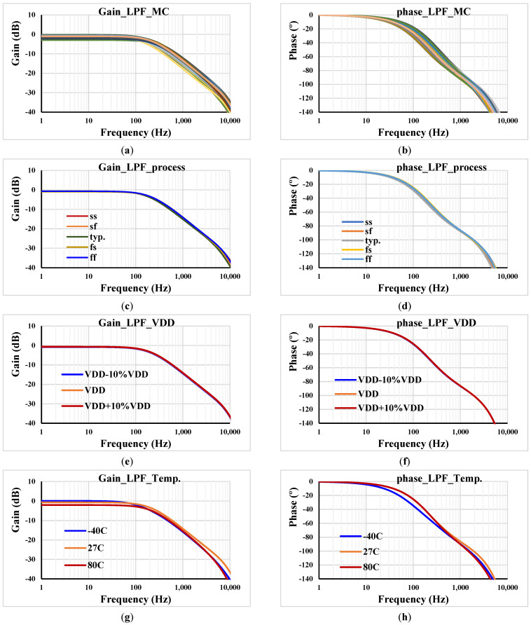
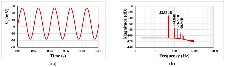
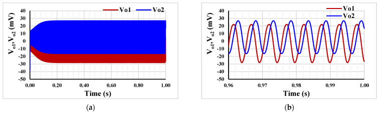
This paper presents a versatile first-order analog filter using differential difference transconductance amplifiers (DDTAs). The DDTA employs the bulk-driven (BD) multiple-input MOS transistors technique (MI-MOST) operating in the subthreshold region. This results in low-voltage and low-power operational capability. Therefore, the DDTA, designed using 130 nm CMOS technology from UMC in the Cadence environment, operates with 0.3 V and consumes 357.4 nW. Unlike previous works, the proposed versatile first-order analog filter provides first-order transfer functions of low-pass, high-pass, and all-pass filters within a single topology. The non-inverting, inverting, and voltage gain of the transfer functions are available for all filters. Furthermore, the proposed structure provides high-input and low-output impedance, which is required for voltage-mode circuits. The pole frequency and voltage gain of the filters can be electronically controlled. The total harmonic distortion of the low-pass filter was calculated as -39.97 dB with an applied sine wave input signal of 50 mV@ 50 Hz. The proposed filter has been used to realize a quadrature oscillator to confirm the advantages of the new structure.
本文提出了一种使用差分差分跨导放大器(DDTA)的多功能一阶模拟滤波器。DDTA 采用在亚阈值区工作的体偏置(BD)多输入 MOS 晶体管技术(MI-MOST)。这使得它具有低压和低功耗的工作能力。因此,采用 UMC 的 130nm CMOS 技术在 Cadence 环境下设计的 DDTA,在 0.3V 下工作,消耗 357.4nW。与以往的工作不同,所提出的多功能一阶模拟滤波器在单个拓扑中提供了低通、高通和全通滤波器的一阶传递函数。所有滤波器都具有非反相、反相和传递函数的电压增益。此外,所提出的结构提供了电压模式电路所需的高输入和低输出阻抗。滤波器的极点频率和电压增益可以进行电子控制。低通滤波器的总谐波失真计算为-39.97dB,施加的正弦波输入信号为 50mV@50Hz。该滤波器已被用于实现正交振荡器,以验证新结构的优势。