Simeonov Simeon, Szekeres Anna, Covei Maria, Stroescu Hermine, Nicolescu Madalina, Chesler Paul, Hornoiu Cristian, Gartner Mariuca
Institute of Solid State Physics, 72, Tsarigradsko Chaussee, 1784 Sofia, Bulgaria.
Department of Product Design, Mechatronics and Environment, Transilvania University of Brasov, 29 Eroilor Bd., 500036 Brasov, Romania.
Materials (Basel). 2024 Apr 22;17(8):1923. doi: 10.3390/ma17081923.
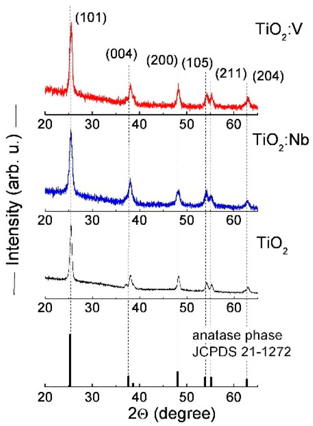
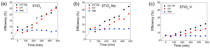
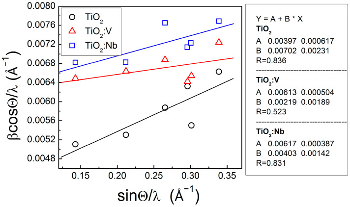
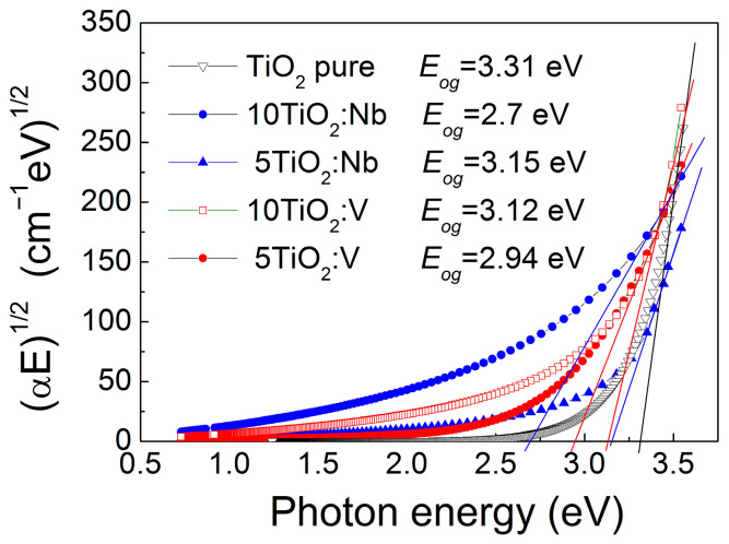
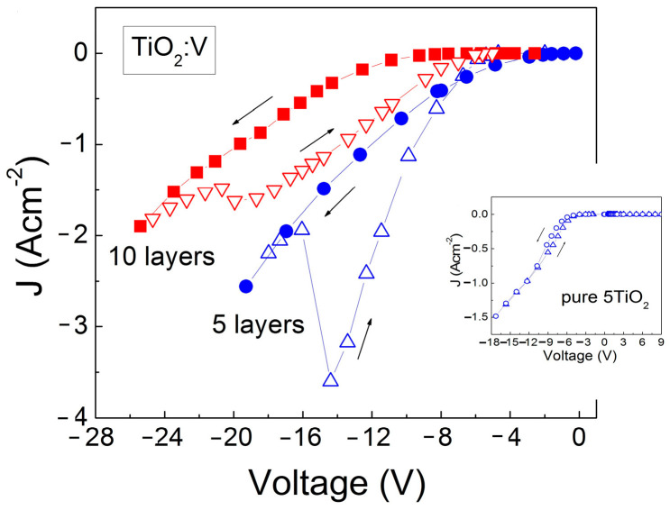
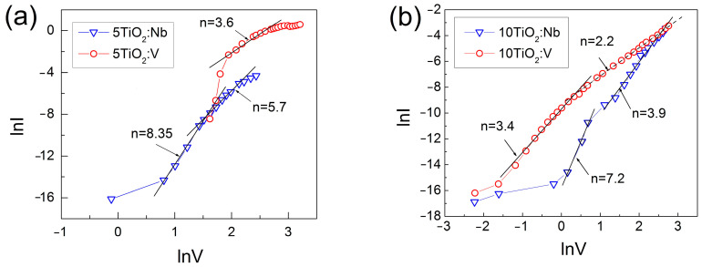
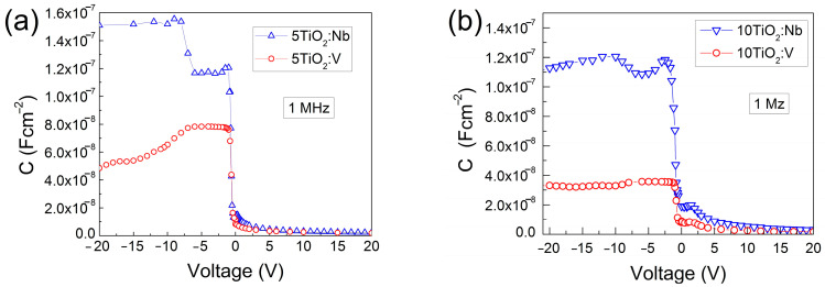
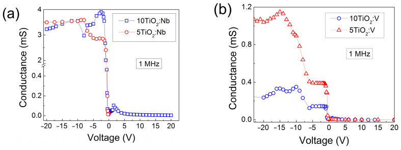
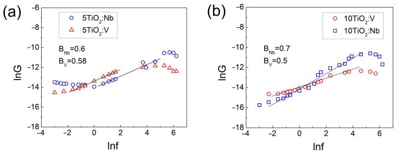
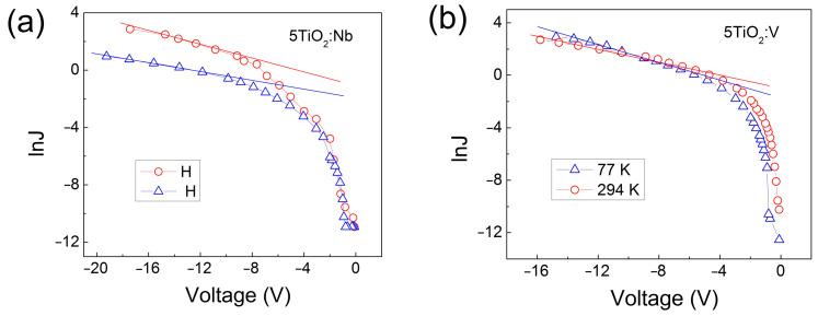
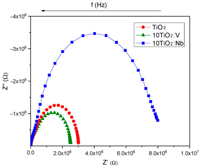
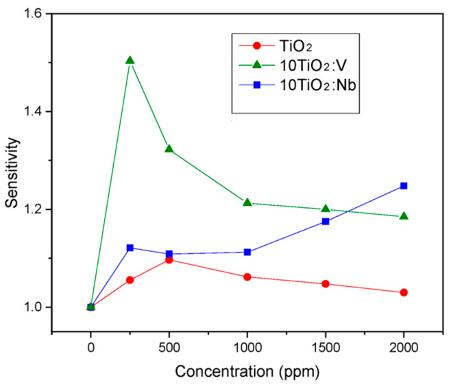
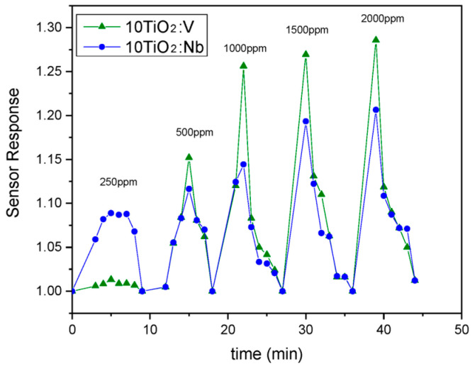
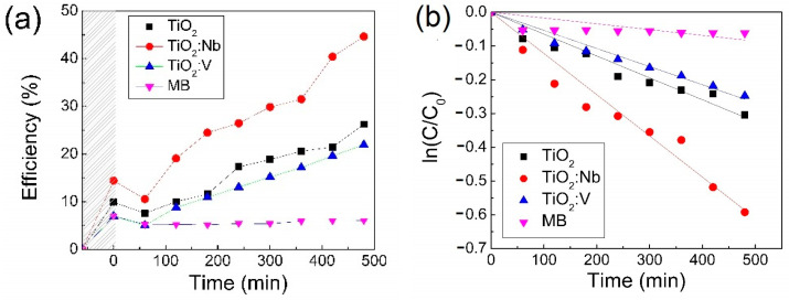
Multilayered TiO films doped either with Niobium or Vanadium (1.2 at. %) were deposited by the sol-gel dip coating method on c-Si and glass substrates. The films on glass substrates were tested for CO sensing and photocatalytic degradation of methylene blue. X-ray diffraction data analysis showed that all the TiO:Nb(V) films were nanocrystalline in the anatase phase, with a uniform and compact microstructure and a homogeneous superficial structure of small grains with diameters in the range of 13-19 nm. For the electrical characterization, the TiO:Nb(V) films were incorporated in Metal-Insulator-Semiconductor (MIS) structures. The specific resistivity is of the order of 10 Ωcm and its value decreases with increasing the electrical field, which testifies to the injection of electrons into these layers. From the analysis of the current-voltage curves taken at different temperature- and frequency-dependent capacitance-voltage and conductance-voltage characteristics, the density and parameters of deep levels in these TiO films are evaluated and the electron charge transport mechanism is established. It was shown that the current in these TiO:Nb(V)-Si MIS structures is mainly carried out by inter-trap tunneling via deep levels energetically distributed in the TiO bandgap. Testing these sol-gel TiO:Nb(V) layers for gas sensing and photocatalytic capabilities proved that they could serve such purposes. In particular, the results of the V-doped sol-gel TiO film confirm its CO detection capability, which is rarely reported in the literature. For the photodegradation of methylene blue, the Nb-doped TiO samples were superior, with nearly double the photocatalytic efficiency of undoped TiO.
采用溶胶 - 凝胶浸涂法在c - Si和玻璃基板上沉积了掺杂铌或钒(1.2原子百分比)的多层TiO薄膜。对玻璃基板上的薄膜进行了CO传感和亚甲基蓝光催化降解测试。X射线衍射数据分析表明,所有TiO:Nb(V)薄膜均为锐钛矿相纳米晶,具有均匀致密的微观结构和直径在13 - 19 nm范围内的小晶粒均匀表面结构。为了进行电学表征,将TiO:Nb(V)薄膜集成到金属 - 绝缘体 - 半导体(MIS)结构中。比电阻率约为10 Ωcm,其值随电场增加而降低,这证明有电子注入到这些层中。通过分析在不同温度和频率下的电容 - 电压及电导 - 电压特性所测得的电流 - 电压曲线,评估了这些TiO薄膜中深能级的密度和参数,并建立了电子电荷传输机制。结果表明,这些TiO:Nb(V) - Si MIS结构中的电流主要通过TiO带隙中能量分布的深能级间的陷阱隧穿来传导。对这些溶胶 - 凝胶TiO:Nb(V)层进行气体传感和光催化性能测试证明它们可用于此类目的。特别是,掺钒溶胶 - 凝胶TiO薄膜的结果证实了其CO检测能力,这在文献中很少报道。对于亚甲基蓝的光降解,掺铌TiO样品表现更优,其光催化效率几乎是未掺杂TiO的两倍。