Danilewsky Andreas, Wittge Jochen, Kiefl Konstantin, Allen David, McNally Patrick, Garagorri Jorge, Elizalde M Reyes, Baumbach Tilo, Tanner Brian K
Kristallographie, Institut für Geowissenschaften, University Freiburg, D-79104, Germany.
J Appl Crystallogr. 2013 Aug 1;46(Pt 4):849-855. doi: 10.1107/S0021889813003695. Epub 2013 Jun 7.
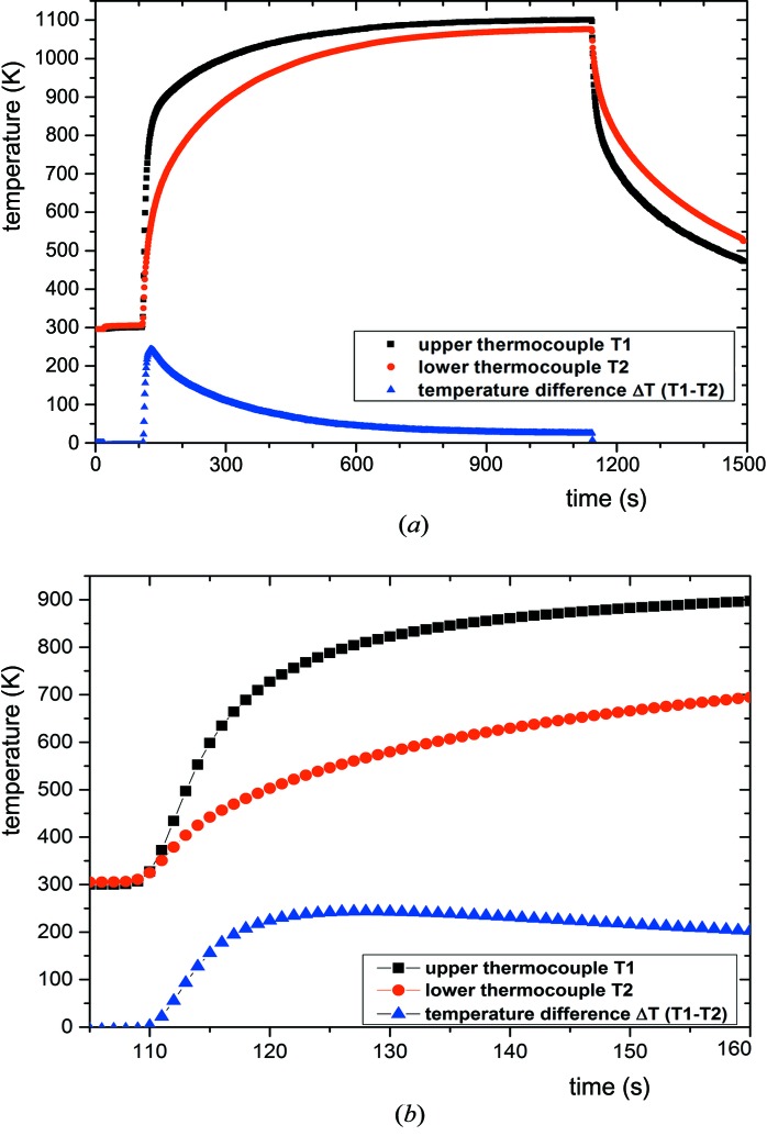
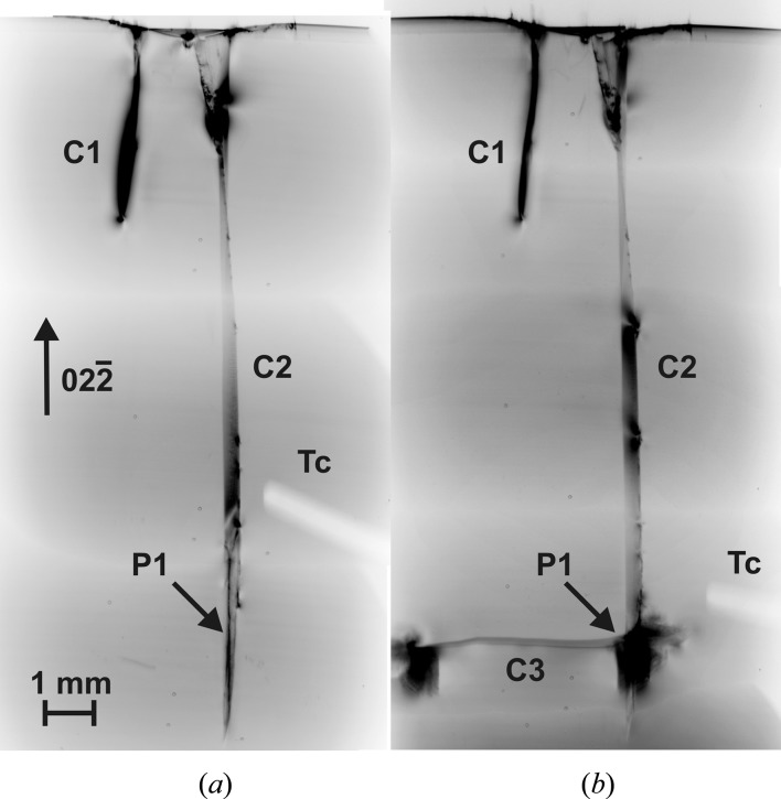
The behaviour of microcracks in silicon during thermal annealing has been studied using X-ray diffraction imaging. Initial cracks are produced with an indenter at the edge of a conventional Si wafer, which was heated under temperature gradients to produce thermal stress. At temperatures where Si is still in the brittle regime, the strain may accumulate if a microcrack is pinned. If a critical value is exceeded either a new or a longer crack will be formed, which results with high probability in wafer breakage. The strain reduces most efficiently by forming () or () crack planes of high energy instead of the expected low-energy cleavage planes like {111}. Dangerous cracks, which become active during heat treatment and may shatter the whole wafer, can be identified from diffraction images simply by measuring the geometrical dimensions of the strain-related contrast around the crack tip. Once the plastic regime at higher temperature is reached, strain is reduced by generating dislocation loops and slip bands and no wafer breakage occurs. There is only a small temperature window within which crack propagation is possible during rapid annealing.
利用X射线衍射成像技术研究了硅在热退火过程中微裂纹的行为。在传统硅片边缘用压头产生初始裂纹,该硅片在温度梯度下加热以产生热应力。在硅仍处于脆性状态的温度下,如果微裂纹被固定,应变可能会积累。如果超过临界值,将形成新的或更长的裂纹,这很可能导致晶片破裂。通过形成高能的()或()裂纹面而不是预期的低能解理面{111},应变能最有效地降低。通过简单地测量裂纹尖端周围与应变相关的对比度的几何尺寸,就可以从衍射图像中识别出在热处理过程中变得活跃并可能使整个晶片破碎的危险裂纹。一旦达到较高温度下的塑性状态,通过产生位错环和滑移带来降低应变,并且不会发生晶片破裂。在快速退火过程中,只有一个很小的温度窗口,在此窗口内裂纹可能扩展。