• 文献检索
  • 文档翻译
  • 深度研究
  • 学术资讯
  • Suppr Zotero 插件Zotero 插件
  • 邀请有礼
  • 套餐&价格
  • 历史记录
应用&插件
Suppr Zotero 插件Zotero 插件浏览器插件Mac 客户端Windows 客户端微信小程序
定价
高级版会员购买积分包购买API积分包
服务
文献检索文档翻译深度研究API 文档MCP 服务
关于我们
关于 Suppr公司介绍联系我们用户协议隐私条款
关注我们

Suppr 超能文献

核心技术专利:CN118964589B侵权必究
粤ICP备2023148730 号-1Suppr @ 2026

文献检索

告别复杂PubMed语法,用中文像聊天一样搜索,搜遍4000万医学文献。AI智能推荐,让科研检索更轻松。

立即免费搜索

文件翻译

保留排版,准确专业,支持PDF/Word/PPT等文件格式,支持 12+语言互译。

免费翻译文档

深度研究

AI帮你快速写综述,25分钟生成高质量综述,智能提取关键信息,辅助科研写作。

立即免费体验

具有高光响应的单晶二维GaSe晶体的可控气相生长。

Controlled vapor phase growth of single crystalline, two-dimensional GaSe crystals with high photoresponse.

作者信息

Li Xufan, Lin Ming-Wei, Puretzky Alexander A, Idrobo Juan C, Ma Cheng, Chi Miaofang, Yoon Mina, Rouleau Christopher M, Kravchenko Ivan I, Geohegan David B, Xiao Kai

机构信息

Center for Nanophase Materials Sciences, Oak Ridge National Laboratory, One Bethel Valley Road, Oak Ridge, TN, 37831, USA.

出版信息

Sci Rep. 2014 Jun 30;4:5497. doi: 10.1038/srep05497.

DOI:10.1038/srep05497
PMID:24975226
原文链接:https://pmc.ncbi.nlm.nih.gov/articles/PMC4074793/
Abstract

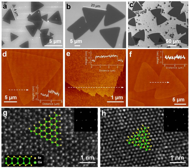
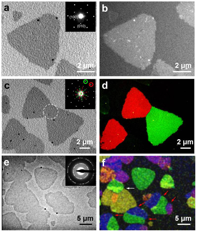
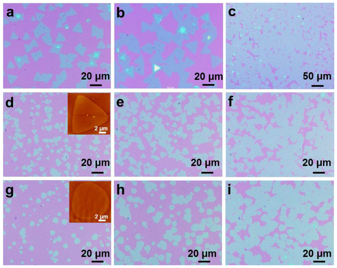
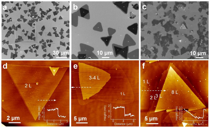
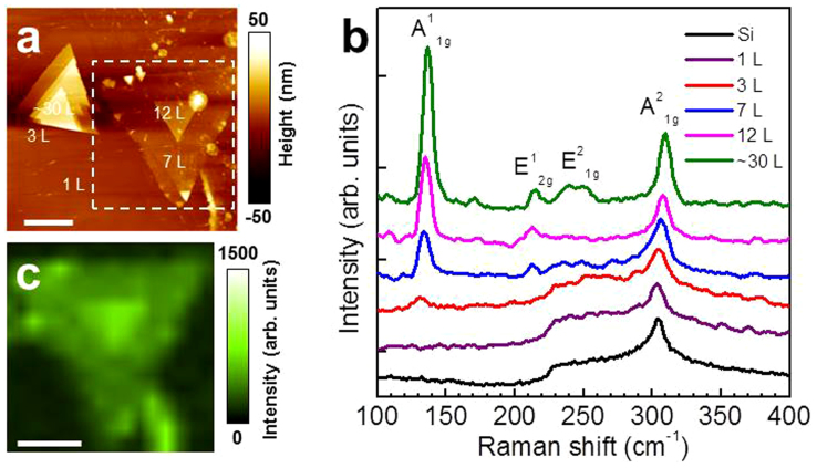
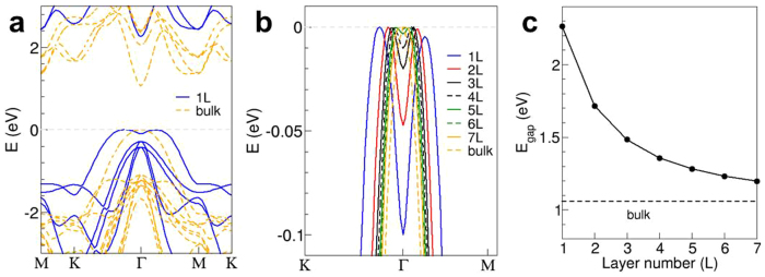
Compared with their bulk counterparts, atomically thin two-dimensional (2D) crystals exhibit new physical properties, and have the potential to enable next-generation electronic and optoelectronic devices. However, controlled synthesis of large uniform monolayer and multi-layer 2D crystals is still challenging. Here, we report the controlled synthesis of 2D GaSe crystals on SiO2/Si substrates using a vapor phase deposition method. For the first time, uniform, large (up to 60 μm in lateral size), single-crystalline, triangular monolayer GaSe crystals were obtained and their structure and orientation were characterized from atomic scale to micrometer scale. The size, density, shape, thickness, and uniformity of the 2D GaSe crystals were shown to be controllable by growth duration, growth region, growth temperature, and argon carrier gas flow rate. The theoretical modeling of the electronic structure and Raman spectroscopy demonstrate a direct-to-indirect bandgap transition and progressive confinement-induced bandgap shifts for 2D GaSe crystals. The 2D GaSe crystals show p-type semiconductor characteristics and high photoresponsivity (1.7 A/W under white light illumination) comparable to exfoliated GaSe nanosheets. These 2D GaSe crystals are potentially useful for next-generation electronic and optoelectronic devices such as photodetectors and field-effect transistors.

摘要

与体相材料相比,原子级薄的二维(2D)晶体展现出了新的物理特性,并且有潜力应用于下一代电子和光电器件。然而,可控合成大面积均匀的单层和多层二维晶体仍然具有挑战性。在此,我们报道了一种利用气相沉积法在SiO2/Si衬底上可控合成二维GaSe晶体的方法。首次获得了均匀、大面积(横向尺寸可达约60μm)、单晶的三角形单层GaSe晶体,并从原子尺度到微米尺度对其结构和取向进行了表征。结果表明,二维GaSe晶体的尺寸、密度、形状、厚度和均匀性可通过生长时间、生长区域、生长温度和氩载气流量来控制。电子结构的理论建模和拉曼光谱表明,二维GaSe晶体存在直接带隙到间接带隙的转变以及由限制效应导致的带隙逐渐移动。二维GaSe晶体表现出p型半导体特性以及高光响应性(白光照射下约为1.7 A/W),与剥离的GaSe纳米片相当。这些二维GaSe晶体在诸如光电探测器和场效应晶体管等下一代电子和光电器件中具有潜在应用价值。

https://cdn.ncbi.nlm.nih.gov/pmc/blobs/5771/4074793/d79d602cb7ad/srep05497-f7.jpg
https://cdn.ncbi.nlm.nih.gov/pmc/blobs/5771/4074793/dd62e4779cfc/srep05497-f1.jpg
https://cdn.ncbi.nlm.nih.gov/pmc/blobs/5771/4074793/91477f4d04fa/srep05497-f2.jpg
https://cdn.ncbi.nlm.nih.gov/pmc/blobs/5771/4074793/78da3ffa0323/srep05497-f3.jpg
https://cdn.ncbi.nlm.nih.gov/pmc/blobs/5771/4074793/e8a2843367f6/srep05497-f4.jpg
https://cdn.ncbi.nlm.nih.gov/pmc/blobs/5771/4074793/fcca836a3f6c/srep05497-f5.jpg
https://cdn.ncbi.nlm.nih.gov/pmc/blobs/5771/4074793/e44eff345b4b/srep05497-f6.jpg
https://cdn.ncbi.nlm.nih.gov/pmc/blobs/5771/4074793/d79d602cb7ad/srep05497-f7.jpg

相似文献

1
Controlled vapor phase growth of single crystalline, two-dimensional GaSe crystals with high photoresponse.具有高光响应的单晶二维GaSe晶体的可控气相生长。
Sci Rep. 2014 Jun 30;4:5497. doi: 10.1038/srep05497.
2
Epitaxy and photoresponse of two-dimensional GaSe crystals on flexible transparent mica sheets.二维 GaSe 晶体在柔性透明云母片上的外延生长和光响应。
ACS Nano. 2014 Feb 25;8(2):1485-90. doi: 10.1021/nn405529r. Epub 2014 Jan 8.
3
Van der Waals Epitaxial Growth of Two-Dimensional Single-Crystalline GaSe Domains on Graphene.范德华外延生长二维单晶 GaSe 畴在石墨烯上。
ACS Nano. 2015 Aug 25;9(8):8078-88. doi: 10.1021/acsnano.5b01943. Epub 2015 Jul 29.
4
Quasi-Van der Waals Epitaxial Growth of γ'-GaSe Nanometer-Thick Films on GaAs(111)B Substrates.γ'-GaSe纳米厚膜在GaAs(111)B衬底上的准范德华外延生长
ACS Nano. 2024 Jul 2;18(26):17185-17196. doi: 10.1021/acsnano.4c04194. Epub 2024 Jun 13.
5
Edge-Controlled Growth and Etching of Two-Dimensional GaSe Monolayers.二维 GaSe 单层的边缘控制生长和刻蚀。
J Am Chem Soc. 2017 Jan 11;139(1):482-491. doi: 10.1021/jacs.6b11076. Epub 2016 Dec 20.
6
Synthesis and photoresponse of large GaSe atomic layers.GaSe 原子层的合成与光响应。
Nano Lett. 2013 Jun 12;13(6):2777-81. doi: 10.1021/nl4010089. Epub 2013 Jun 3.
7
Synthesis of few-layer GaSe nanosheets for high performance photodetectors.用于高性能光探测器的少层 GaSe 纳米片的合成。
ACS Nano. 2012 Jul 24;6(7):5988-94. doi: 10.1021/nn300889c. Epub 2012 Jun 7.
8
Layer-independent and layer-dependent nonlinear optical properties of two-dimensional GaX (X = S, Se, Te) nanosheets.二维GaX(X = S、Se、Te)纳米片的与层数无关和与层数有关的非线性光学性质。
Phys Chem Chem Phys. 2017 May 10;19(18):11131-11141. doi: 10.1039/c7cp00578d.
9
Thickness dependence on the optoelectronic properties of multilayered GaSe based photodetector.多层 GaSe 基光电探测器光电性能的厚度依赖性。
Nanotechnology. 2016 Aug 12;27(32):325202. doi: 10.1088/0957-4484/27/32/325202. Epub 2016 Jun 29.
10
Synthetic Control of Two-Dimensional NiTe Single Crystals with Highly Uniform Thickness Distributions.具有高度均匀厚度分布的二维NiTe单晶的合成控制。
J Am Chem Soc. 2018 Oct 31;140(43):14217-14223. doi: 10.1021/jacs.8b08124. Epub 2018 Oct 22.

引用本文的文献

1
Electronic Band Structure of Gallium Sulfide (GaS) with Thickness Reduction Unveiling Parabolic and Pudding Mold Band Dispersion.硫化镓(GaS)厚度减小后的电子能带结构揭示抛物线型和布丁模型能带色散
J Phys Chem C Nanomater Interfaces. 2025 Feb 5;129(7):3967-3974. doi: 10.1021/acs.jpcc.4c08588. eCollection 2025 Feb 20.
2
Probing and manipulating the Mexican hat-shaped valence band of InSe.探测和操控硒化铟的墨西哥帽形价带。
Nat Commun. 2025 Jan 22;16(1):922. doi: 10.1038/s41467-025-56139-8.
3
Tunable Electronic Properties of Two-Dimensional GaSeTe Alloys.

本文引用的文献

1
Evolution of the electronic band structure and efficient photo-detection in atomic layers of InSe.InSe 原子层中电子能带结构的演化和高效光探测。
ACS Nano. 2014 Feb 25;8(2):1263-72. doi: 10.1021/nn405036u. Epub 2014 Jan 13.
2
Controlled growth of high-quality monolayer WS2 layers on sapphire and imaging its grain boundary.在蓝宝石上控制高质量单层 WS2 层的生长并对其晶界进行成像。
ACS Nano. 2013 Oct 22;7(10):8963-71. doi: 10.1021/nn403454e. Epub 2013 Sep 24.
3
Tuning the bandgap of exfoliated InSe nanosheets by quantum confinement.
二维GaSeTe合金的可调电子性质
Nanomaterials (Basel). 2023 Feb 23;13(5):818. doi: 10.3390/nano13050818.
4
Controllable Thin-Film Approaches for Doping and Alloying Transition Metal Dichalcogenides Monolayers.用于掺杂和合金化过渡金属二硫属化物单层的可控薄膜方法。
Adv Sci (Weinh). 2021 Feb 26;8(9):2004249. doi: 10.1002/advs.202004249. eCollection 2021 May.
5
Substrate-induced strain in 2D layered GaSe materials grown by molecular beam epitaxy.分子束外延生长的二维层状GaSe材料中的衬底诱导应变。
Sci Rep. 2020 Jul 31;10(1):12972. doi: 10.1038/s41598-020-69946-4.
6
Asymmetric electrode incorporated 2D GeSe for self-biased and efficient photodetection.用于自偏置高效光电探测的不对称电极集成二维GeSe
Sci Rep. 2020 Jun 10;10(1):9374. doi: 10.1038/s41598-020-66263-8.
7
Screw-Dislocation-Driven Growth Mode in Two Dimensional GaSe on GaAs(001) Substrates Grown by Molecular Beam Epitaxy.分子束外延生长在GaAs(001)衬底上的二维GaSe中的螺旋位错驱动生长模式
Sci Rep. 2019 Nov 28;9(1):17781. doi: 10.1038/s41598-019-54406-5.
8
Thermoelectric Performance of Two-Dimensional AlX (X = S, Se, Te): A First-Principles-Based Transport Study.二维AlX(X = S、Se、Te)的热电性能:基于第一性原理的输运研究
ACS Omega. 2019 Oct 17;4(18):17773-17781. doi: 10.1021/acsomega.9b02235. eCollection 2019 Oct 29.
9
Photoresponse of Graphene-Gated Graphene-GaSe Heterojunction Devices.石墨烯栅控石墨烯-硒化镓异质结器件的光响应
ACS Appl Nano Mater. 2018 Aug 24;1(8):3895-3902. doi: 10.1021/acsanm.8b00684. Epub 2018 Jul 31.
10
Abnormal band bowing effects in phase instability crossover region of GaSeTe nanomaterials.GaSeTe 纳米材料中相不稳定性交叉区域的异常能带弯曲效应。
Nat Commun. 2018 May 15;9(1):1927. doi: 10.1038/s41467-018-04328-z.
通过量子限域来调节剥离的 InSe 纳米片的带隙。
Adv Mater. 2013 Oct 25;25(40):5714-8. doi: 10.1002/adma.201302616. Epub 2013 Aug 21.
4
Optical generation of excitonic valley coherence in monolayer WSe2.单层 WSe2 中激子谷相干的光激发。
Nat Nanotechnol. 2013 Sep;8(9):634-8. doi: 10.1038/nnano.2013.151. Epub 2013 Aug 11.
5
Vapour phase growth and grain boundary structure of molybdenum disulphide atomic layers.二硫化钼原子层的蒸气相生长和晶界结构。
Nat Mater. 2013 Aug;12(8):754-9. doi: 10.1038/nmat3673. Epub 2013 Jun 9.
6
Synthesis and photoresponse of large GaSe atomic layers.GaSe 原子层的合成与光响应。
Nano Lett. 2013 Jun 12;13(6):2777-81. doi: 10.1021/nl4010089. Epub 2013 Jun 3.
7
Grains and grain boundaries in highly crystalline monolayer molybdenum disulphide.高度结晶的单层二硫化钼中的晶粒和晶界。
Nat Mater. 2013 Jun;12(6):554-61. doi: 10.1038/nmat3633. Epub 2013 May 5.
8
Tunable electronic and dielectric behavior of GaS and GaSe monolayers.可调谐的 GaS 和 GaSe 单层的电子和介电性能。
Phys Chem Chem Phys. 2013 May 21;15(19):7098-105. doi: 10.1039/c3cp50233c.
9
The chemistry of two-dimensional layered transition metal dichalcogenide nanosheets.二维层状过渡金属二卤化物纳米片的化学。
Nat Chem. 2013 Apr;5(4):263-75. doi: 10.1038/nchem.1589.
10
Synthesis and transfer of single-layer transition metal disulfides on diverse surfaces.单层过渡金属二硫化物在多种表面上的合成与转移。
Nano Lett. 2013 Apr 10;13(4):1852-7. doi: 10.1021/nl400687n. Epub 2013 Mar 29.