• 文献检索
  • 文档翻译
  • 深度研究
  • 学术资讯
  • Suppr Zotero 插件Zotero 插件
  • 邀请有礼
  • 套餐&价格
  • 历史记录
应用&插件
Suppr Zotero 插件Zotero 插件浏览器插件Mac 客户端Windows 客户端微信小程序
定价
高级版会员购买积分包购买API积分包
服务
文献检索文档翻译深度研究API 文档MCP 服务
关于我们
关于 Suppr公司介绍联系我们用户协议隐私条款
关注我们

Suppr 超能文献

核心技术专利:CN118964589B侵权必究
粤ICP备2023148730 号-1Suppr @ 2026

文献检索

告别复杂PubMed语法,用中文像聊天一样搜索,搜遍4000万医学文献。AI智能推荐,让科研检索更轻松。

立即免费搜索

文件翻译

保留排版,准确专业,支持PDF/Word/PPT等文件格式,支持 12+语言互译。

免费翻译文档

深度研究

AI帮你快速写综述,25分钟生成高质量综述,智能提取关键信息,辅助科研写作。

立即免费体验

使用等离子体电极的超快非接触式快速烧结

Ultrafast-Contactless Flash Sintering using Plasma Electrodes.

作者信息

Saunders Theo, Grasso Salvatore, Reece Michael J

机构信息

School of Engineering and Material Science, Queen Mary University of London, London, E1 4NS, UK.

出版信息

Sci Rep. 2016 Jun 8;6:27222. doi: 10.1038/srep27222.

DOI:10.1038/srep27222
PMID:27273255
原文链接:https://pmc.ncbi.nlm.nih.gov/articles/PMC4897693/
Abstract

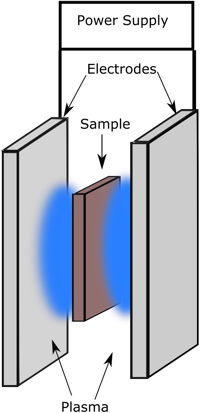
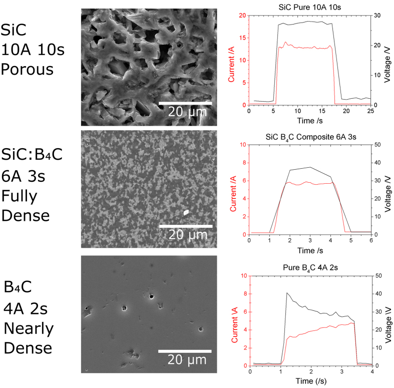
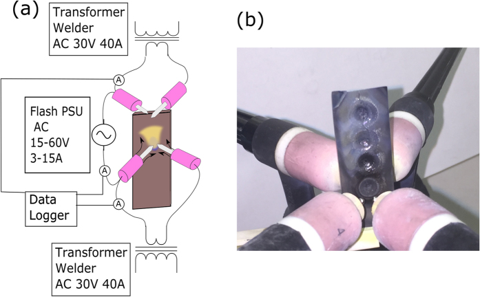
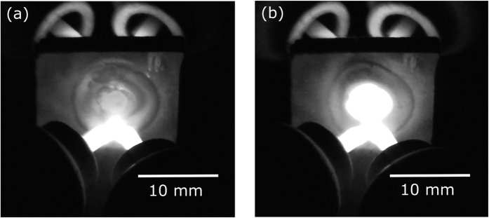
This paper presents a novel derivative of flash sintering, in which contactless flash sintering (CFS) is achieved using plasma electrodes. In this setup, electrical contact with the sample to be sintered is made by two arc plasma electrodes, one on either side, allowing current to pass through the sample. This opens up the possibility of continuous throughput flash sintering. Preheating, a usual precondition for flash sintering, is provided by the arc electrodes which heat the sample to 1400 °C. The best results were produced with pre-compacted samples (bars 1.8 mm thick) of pure B4C (discharge time 2s, current 4A) and SiC:B4C 50 wt% (3s at 6A), which were fully consolidated under a heating rate approaching 20000 °C/min. For the composite a cylindrical volume of 14 mm(3) was sintered to full density with limited grain growth.

摘要

本文介绍了一种新型的快速烧结衍生物,即通过等离子体电极实现非接触式快速烧结(CFS)。在这种装置中,通过两个电弧等离子体电极与待烧结样品进行电接触,两侧各一个,使电流通过样品。这为连续通量快速烧结开辟了可能性。电弧电极提供了快速烧结通常所需的预热条件,将样品加热到1400°C。纯B4C预压实样品(1.8毫米厚的棒材,放电时间2秒,电流4A)和50 wt% SiC:B4C(6A下3秒)取得了最佳结果,它们在接近20000°C/分钟的加热速率下完全固结。对于该复合材料,14立方毫米的圆柱体积被烧结至全密度,且晶粒生长有限。

https://cdn.ncbi.nlm.nih.gov/pmc/blobs/2a9e/4897693/f3620b1f54fd/srep27222-f4.jpg
https://cdn.ncbi.nlm.nih.gov/pmc/blobs/2a9e/4897693/72d0e13e7014/srep27222-f1.jpg
https://cdn.ncbi.nlm.nih.gov/pmc/blobs/2a9e/4897693/0c74293b4317/srep27222-f2.jpg
https://cdn.ncbi.nlm.nih.gov/pmc/blobs/2a9e/4897693/1d62d743538d/srep27222-f3.jpg
https://cdn.ncbi.nlm.nih.gov/pmc/blobs/2a9e/4897693/f3620b1f54fd/srep27222-f4.jpg

相似文献

1
Ultrafast-Contactless Flash Sintering using Plasma Electrodes.使用等离子体电极的超快非接触式快速烧结
Sci Rep. 2016 Jun 8;6:27222. doi: 10.1038/srep27222.
2
Formation of secondary phase at grain boundary of flash-sintered BaTiO3.快速烧结的钛酸钡晶界处第二相的形成。
Microscopy (Oxf). 2014 Nov;63 Suppl 1:i19-i20. doi: 10.1093/jmicro/dfu048.
3
Flash (Ultra-Rapid) Spark-Plasma Sintering of Silicon Carbide.闪烧(超快速)火花等离子体烧结碳化硅。
Sci Rep. 2016 Sep 14;6:33408. doi: 10.1038/srep33408.
4
A simple flash sintering setup under applied mechanical stress and controlled atmosphere.一种在施加机械应力和可控气氛下的简单快速烧结装置。
MethodsX. 2015 Oct 17;2:392-8. doi: 10.1016/j.mex.2015.10.004. eCollection 2015.
5
Sintering Behavior of Spark Plasma Sintered SiC with Si-SiC Composite Nanoparticles Prepared by Thermal DC Plasma Process.热直流等离子体法制备的含Si-SiC复合纳米颗粒的放电等离子烧结SiC的烧结行为
Nanoscale Res Lett. 2017 Nov 25;12(1):606. doi: 10.1186/s11671-017-2370-8.
6
Photonic Flash Sintering of Ink-Jet-Printed Back Electrodes for Organic Photovoltaic Applications.用于有机光伏应用的喷墨打印背电极的光闪烧结。
ACS Appl Mater Interfaces. 2016 Jan 27;8(3):2325-35. doi: 10.1021/acsami.5b11394. Epub 2016 Jan 12.
7
On the Mechanism of Microwave Flash Sintering of Ceramics.陶瓷微波快速烧结机理研究
Materials (Basel). 2016 Aug 11;9(8):684. doi: 10.3390/ma9080684.
8
In situ monitoring of a flash light sintering process using silver nano-ink for producing flexible electronics.利用银纳米墨水进行闪光烧结过程的原位监测,以生产柔性电子产品。
Nanotechnology. 2013 Jan 25;24(3):035202. doi: 10.1088/0957-4484/24/3/035202. Epub 2012 Dec 21.
9
Intensive Plasmonic Flash Light Sintering of Copper Nanoinks Using a Band-Pass Light Filter for Highly Electrically Conductive Electrodes in Printed Electronics.采用带通滤光片的密集等离子体闪光烧结铜纳米油墨,用于印刷电子中高导电性电极。
ACS Appl Mater Interfaces. 2016 Apr 6;8(13):8591-9. doi: 10.1021/acsami.5b12516. Epub 2016 Mar 28.
10
Ultrahigh Temperature Flash Sintering of Binder-Less Tungsten Carbide within 6 s.无粘结剂碳化钨在6秒内的超高温快速烧结
Materials (Basel). 2021 Dec 12;14(24):7655. doi: 10.3390/ma14247655.

引用本文的文献

1
Flash Sintering Research Perspective: A Bibliometric Analysis.快速烧结研究视角:文献计量分析
Materials (Basel). 2022 Jan 6;15(2):416. doi: 10.3390/ma15020416.
2
Spark Plasma Sintered BC-Structural, Thermal, Electrical and Mechanical Properties.放电等离子烧结的BC结构、热学、电学和力学性能
Materials (Basel). 2020 Apr 1;13(7):1612. doi: 10.3390/ma13071612.
3
All-Materials-Inclusive Flash Spark Plasma Sintering.全材料包容式快速火花等离子烧结

本文引用的文献

1
Sintering of CuO and ZnO in a single mode microwave cavity with shrinkage control.
J Microw Power Electromagn Energy. 2010;44(1):57-63. doi: 10.1080/08327823.2010.11689770.
2
Pressure and temperature dependences of the electronic conductivity of boron carbides.碳化硼电子电导率与压力和温度的关系
Phys Rev B Condens Matter. 1985 Aug 15;32(4):2315-2318. doi: 10.1103/physrevb.32.2315.
Sci Rep. 2017 Nov 8;7(1):15071. doi: 10.1038/s41598-017-15365-x.