Department of Materials Science and State Key Laboratory of Molecular Engineering of Polymers, Fudan University, Shanghai 200433, China.
School of Electronic Engineering, Bangor University, Bangor LL57 1UT, UK.
Sci Adv. 2016 Aug 12;2(8):e1600901. doi: 10.1126/sciadv.1600901. eCollection 2016 Aug.
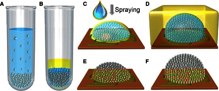
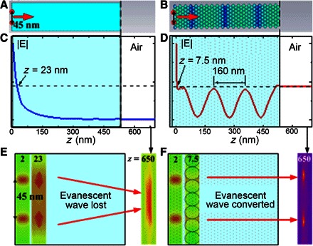
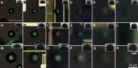
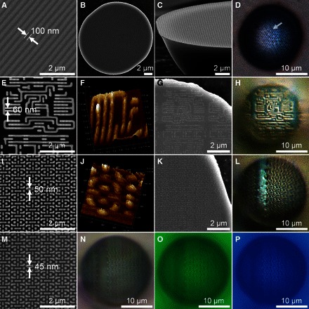
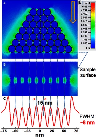
Although all-dielectric metamaterials offer a low-loss alternative to current metal-based metamaterials to manipulate light at the nanoscale and may have important applications, very few have been reported to date owing to the current nanofabrication technologies. We develop a new "nano-solid-fluid assembly" method using 15-nm TiO2 nanoparticles as building blocks to fabricate the first three-dimensional (3D) all-dielectric metamaterial at visible frequencies. Because of its optical transparency, high refractive index, and deep-subwavelength structures, this 3D all-dielectric metamaterial-based solid immersion lens (mSIL) can produce a sharp image with a super-resolution of at least 45 nm under a white-light optical microscope, significantly exceeding the classical diffraction limit and previous near-field imaging techniques. Theoretical analysis reveals that electric field enhancement can be formed between contacting TiO2 nanoparticles, which causes effective confinement and propagation of visible light at the deep-subwavelength scale. This endows the mSIL with unusual abilities to illuminate object surfaces with large-area nanoscale near-field evanescent spots and to collect and convert the evanescent information into propagating waves. Our all-dielectric metamaterial design strategy demonstrates the potential to develop low-loss nanophotonic devices at visible frequencies.
虽然全电介质超材料为操控纳米尺度的光提供了一种比当前基于金属的超材料更低损耗的选择,并且可能具有重要的应用,但由于当前的纳米制造技术,迄今为止报道的非常少。我们开发了一种新的“纳米固液组装”方法,使用 15nm TiO2 纳米粒子作为构建块,在可见频率下制造出第一个三维(3D)全电介质超材料。由于其光学透明度、高折射率和亚波长结构,这种基于 3D 全电介质超材料的固态浸没透镜(mSIL)可以在白光显微镜下产生具有至少 45nm 超分辨率的清晰图像,显著超过经典的衍射极限和以前的近场成像技术。理论分析表明,在接触的 TiO2 纳米粒子之间可以形成电场增强,这导致可见光在亚波长尺度上的有效限制和传播。这赋予了 mSIL 用大面积纳米级近场消逝场照射物体表面的非凡能力,并收集和转换消逝信息为传播波。我们的全电介质超材料设计策略展示了在可见频率下开发低损耗纳米光子器件的潜力。