College of Metallurgy and Materials Engineering, Chongqing University of Science and Technology, Chongqing Key Laboratory of Nano/Micro Composites and Devices, Chongqing, 401331, China.
International Center for Materials Nanoarchitectonics (WPI-MANA), National Institute for Materials Science (NIMS), Tsukuba, Ibaraki, 305-0044, Japan.
Sci Rep. 2017 Jun 15;7(1):3630. doi: 10.1038/s41598-017-03301-y.
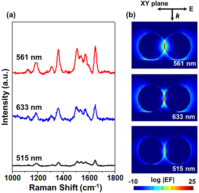
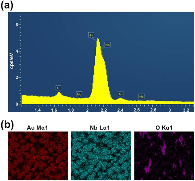
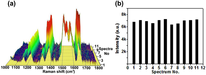
Assemble metal nanoparticles into various ordered structures with scale up to centimeter area is required to meet diverse needs of lab-on-a-chips and analytic components. Here, we present the uniform and high-yield fabrication of centimeter-scale gold nanoparticles (AuNPs) array for SERS substrates. Ferroelectric-assisted assembly of AuNPs line array is successfully fabricated by using a periodically poled LiNbO (PPLN) single crystal as a template. SNOM-Raman shows that the uniform assembly of AuNPs exhibits a high density of "hot spots" arising from strong electromagnetic (EM) field coupling induced by adjacent AuNPs. Quantitative analysis based on SERS detection describes an excellent reproducibility with an intensity variation less than 7% at 1649 cm of Rhodamine 6G. SERS spectra combined with 3D-FDTD modelling indicate that the EM enhancement occurs at all three excitation wavelength of 515, 561 and 633 nm and the 561-nm-laser displays the strongest Raman enhancement with an enhancement factor in an order of 10. The corresponding experimental and theoretical results present a new strategy to fabricate large-area, highly reproducible and sensitive SERS substrates for practical applications.
将金属纳米粒子组装成各种有序结构,其面积可达厘米级,这是满足微流控芯片和分析组件多样化需求所必需的。在这里,我们提出了一种用于 SERS 衬底的厘米级金纳米粒子(AuNPs)阵列的均匀、高产制造方法。通过使用周期性极化 LiNbO(PPLN)单晶体作为模板,成功地制造了铁电辅助组装的 AuNP 线阵。SNOM-Raman 表明,AuNP 的均匀组装表现出高密度的“热点”,这是由相邻 AuNP 引起的强电磁场(EM)耦合产生的。基于 SERS 检测的定量分析描述了 Rhodamine 6G 在 1649cm 处的强度变化小于 7%的优异重现性。SERS 光谱结合 3D-FDTD 模型表明,在所有三个激发波长 515、561 和 633nm 处都发生了 EM 增强,561nm 激光显示出最强的拉曼增强,增强因子在 10 的数量级。相应的实验和理论结果为实际应用提供了一种制造大面积、高重现性和高灵敏度 SERS 衬底的新策略。