• 文献检索
  • 文档翻译
  • 深度研究
  • 学术资讯
  • Suppr Zotero 插件Zotero 插件
  • 邀请有礼
  • 套餐&价格
  • 历史记录
应用&插件
Suppr Zotero 插件Zotero 插件浏览器插件Mac 客户端Windows 客户端微信小程序
定价
高级版会员购买积分包购买API积分包
服务
文献检索文档翻译深度研究API 文档MCP 服务
关于我们
关于 Suppr公司介绍联系我们用户协议隐私条款
关注我们

Suppr 超能文献

核心技术专利:CN118964589B侵权必究
粤ICP备2023148730 号-1Suppr @ 2026

文献检索

告别复杂PubMed语法,用中文像聊天一样搜索,搜遍4000万医学文献。AI智能推荐,让科研检索更轻松。

立即免费搜索

文件翻译

保留排版,准确专业,支持PDF/Word/PPT等文件格式,支持 12+语言互译。

免费翻译文档

深度研究

AI帮你快速写综述,25分钟生成高质量综述,智能提取关键信息,辅助科研写作。

立即免费体验

使用导电SU-8在柔性基板上制造用于传感应用的电路。

Fabrication of Circuits on Flexible Substrates Using Conductive SU-8 for Sensing Applications.

作者信息

Gerardo Carlos D, Cretu Edmond, Rohling Robert

机构信息

Department of Electrical and Computer Engineering, University of British Columbia, Vancouver, BC V6T 1Z4, Canada.

Department of Mechanical Engineering Department, University of British Columbia, Vancouver, BC V6T 1Z4, Canada.

出版信息

Sensors (Basel). 2017 Jun 17;17(6):1420. doi: 10.3390/s17061420.

DOI:10.3390/s17061420
PMID:28629134
原文链接:https://pmc.ncbi.nlm.nih.gov/articles/PMC5492358/
Abstract

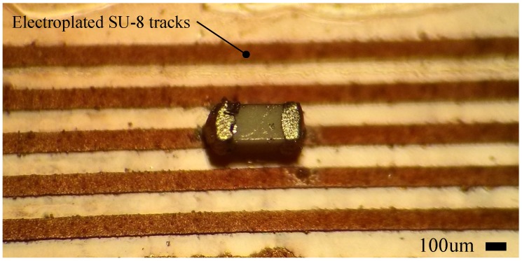
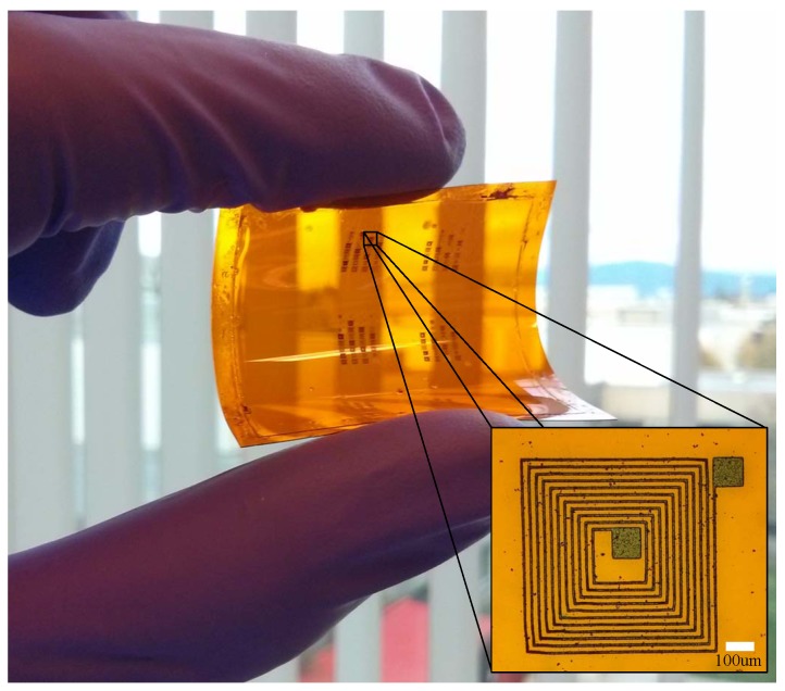
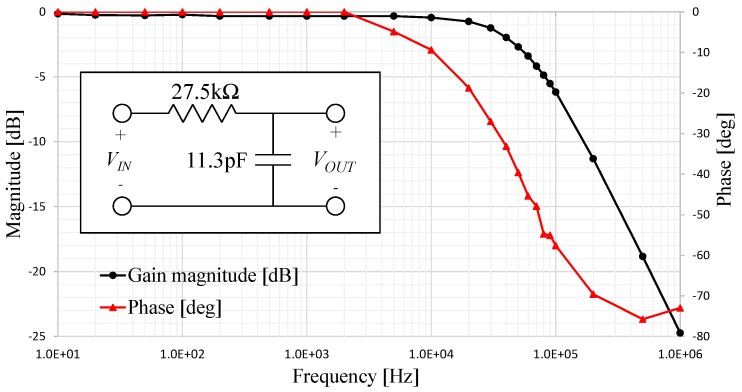
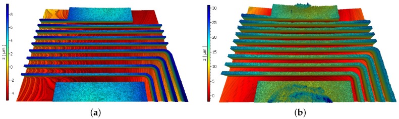
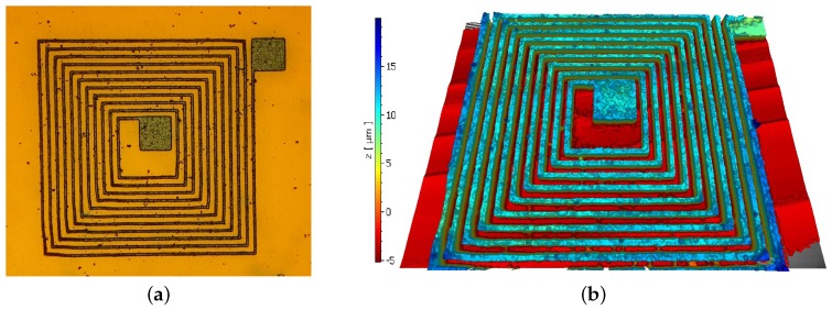
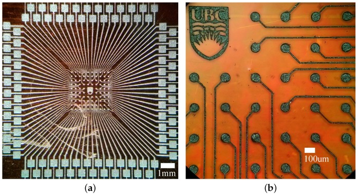
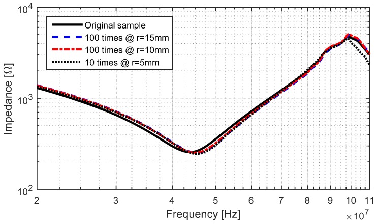
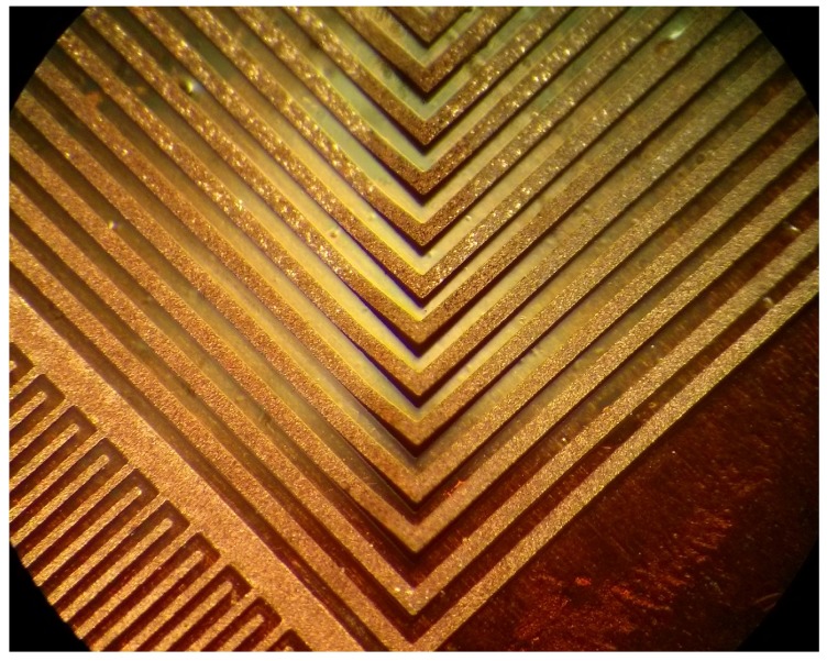
This article describes a new low-cost rapid microfabrication technology for high-density interconnects and passive devices on flexible substrates for sensing applications. Silver nanoparticles with an average size of 80 nm were used to create a conductive SU-8 mixture with a concentration of wt 25%. The patterned structures after hard baking have a sheet resistance of 11.17 Ω /□. This conductive SU-8 was used to pattern planar inductors, capacitors and interconnection lines on flexible Kapton film. The conductive SU-8 structures were used as a seed layer for a subsequent electroplating process to increase the conductivity of the devices. Examples of inductors, resistor-capacitor (RC) and inductor-capacitor (LC) circuits, interconnection lines and a near-field communication (NFC) antenna are presented as a demonstration. As an example of high-resolution miniaturization, we fabricated microinductors having line widths of 5 μ m. Mechanical bending tests were successful down to a 5 mm radius. To the best of the authors' knowledge, this is the first report of conductive SU-8 used to fabricate such planar devices and the first on flexible substrates. This is a proof of concept that this fabrication approach can be used as an alternative for microfabrication of planar passive devices on flexible substrates.

摘要

本文介绍了一种用于传感应用的柔性基板上高密度互连和无源器件的新型低成本快速微制造技术。使用平均尺寸为80nm的银纳米颗粒来制备浓度为25wt%的导电SU-8混合物。硬烘焙后的图案化结构的方块电阻为11.17Ω/□。这种导电SU-8用于在柔性聚酰亚胺薄膜上图案化平面电感器、电容器和互连线。导电SU-8结构用作后续电镀工艺的种子层,以提高器件的导电性。作为示例,展示了电感器、电阻-电容(RC)和电感-电容(LC)电路、互连线以及近场通信(NFC)天线。作为高分辨率小型化的一个例子,我们制造了线宽为5μm的微型电感器。机械弯曲测试在半径低至5mm时仍取得成功。据作者所知,这是关于使用导电SU-8制造此类平面器件的首次报道,也是在柔性基板上的首次报道。这证明了这种制造方法可作为柔性基板上平面无源器件微制造的一种替代方法。

https://cdn.ncbi.nlm.nih.gov/pmc/blobs/704e/5492358/86de8731e3a6/sensors-17-01420-g017.jpg
https://cdn.ncbi.nlm.nih.gov/pmc/blobs/704e/5492358/054383aa2221/sensors-17-01420-g001.jpg
https://cdn.ncbi.nlm.nih.gov/pmc/blobs/704e/5492358/0893ef9c1c97/sensors-17-01420-g002.jpg
https://cdn.ncbi.nlm.nih.gov/pmc/blobs/704e/5492358/657f0acc9bed/sensors-17-01420-g003.jpg
https://cdn.ncbi.nlm.nih.gov/pmc/blobs/704e/5492358/e2d4ef701fd8/sensors-17-01420-g004.jpg
https://cdn.ncbi.nlm.nih.gov/pmc/blobs/704e/5492358/d7d32d322648/sensors-17-01420-g005.jpg
https://cdn.ncbi.nlm.nih.gov/pmc/blobs/704e/5492358/160b567b858d/sensors-17-01420-g006.jpg
https://cdn.ncbi.nlm.nih.gov/pmc/blobs/704e/5492358/67f4dcb518ab/sensors-17-01420-g007.jpg
https://cdn.ncbi.nlm.nih.gov/pmc/blobs/704e/5492358/83a1f18067be/sensors-17-01420-g008.jpg
https://cdn.ncbi.nlm.nih.gov/pmc/blobs/704e/5492358/7e654296bae7/sensors-17-01420-g009.jpg
https://cdn.ncbi.nlm.nih.gov/pmc/blobs/704e/5492358/5dd97aa7c22a/sensors-17-01420-g010.jpg
https://cdn.ncbi.nlm.nih.gov/pmc/blobs/704e/5492358/d2f44aa5269c/sensors-17-01420-g011.jpg
https://cdn.ncbi.nlm.nih.gov/pmc/blobs/704e/5492358/bca2b1d66b2f/sensors-17-01420-g012.jpg
https://cdn.ncbi.nlm.nih.gov/pmc/blobs/704e/5492358/38f723a43ed3/sensors-17-01420-g013.jpg
https://cdn.ncbi.nlm.nih.gov/pmc/blobs/704e/5492358/34bf277c081c/sensors-17-01420-g014.jpg
https://cdn.ncbi.nlm.nih.gov/pmc/blobs/704e/5492358/7e591b4005f9/sensors-17-01420-g015.jpg
https://cdn.ncbi.nlm.nih.gov/pmc/blobs/704e/5492358/f4c08b24eec2/sensors-17-01420-g016.jpg
https://cdn.ncbi.nlm.nih.gov/pmc/blobs/704e/5492358/86de8731e3a6/sensors-17-01420-g017.jpg

相似文献

1
Fabrication of Circuits on Flexible Substrates Using Conductive SU-8 for Sensing Applications.使用导电SU-8在柔性基板上制造用于传感应用的电路。
Sensors (Basel). 2017 Jun 17;17(6):1420. doi: 10.3390/s17061420.
2
Designing Surface Chemistry of Silver Nanocrystals for Radio Frequency Circuit Applications.设计用于射频电路应用的银纳米晶体的表面化学性质。
ACS Appl Mater Interfaces. 2018 Oct 31;10(43):37643-37650. doi: 10.1021/acsami.8b12005. Epub 2018 Oct 17.
3
Selective Electroless Metallization of Micro- and Nanopatterns via Poly(dopamine) Modification and Palladium Nanoparticle Catalysis for Flexible and Stretchable Electronic Applications.通过聚多巴胺改性和钯纳米粒子催化选择性化学镀实现微纳图案化,用于柔性可拉伸电子应用。
ACS Appl Mater Interfaces. 2018 Aug 29;10(34):28754-28763. doi: 10.1021/acsami.8b07411. Epub 2018 Aug 21.
4
Laser-Direct Writing of Silver Metal Electrodes on Transparent Flexible Substrates with High-Bonding Strength.激光直写在具有高结合强度的透明柔性衬底上的银金属电极。
ACS Appl Mater Interfaces. 2016 Sep 21;8(37):24887-92. doi: 10.1021/acsami.6b07696. Epub 2016 Sep 8.
5
Rapid two-step metallization through physicochemical conversion of Ag2O for printed "black" transparent conductive films.通过 Ag2O 的物理化学转化实现快速两步金属化,用于打印“黑色”透明导电薄膜。
Nanoscale. 2013 Jun 7;5(11):5043-52. doi: 10.1039/c3nr00962a. Epub 2013 May 2.
6
The Conductive Silver Nanowires Fabricated by Two-beam Laser Direct Writing on the Flexible Sheet.双光束激光直写在柔性基底上制备的导电银纳米线织物。
Sci Rep. 2017 Feb 2;7:41757. doi: 10.1038/srep41757.
7
Direct Laser Writing of Porous-Carbon/Silver Nanocomposite for Flexible Electronics.直接激光写入多孔碳/银纳米复合材料用于柔性电子。
ACS Appl Mater Interfaces. 2016 Jul 6;8(26):16907-13. doi: 10.1021/acsami.6b02952. Epub 2016 Jun 22.
8
Fabrication of Two-Dimensional and Three-Dimensional High-Resolution Binder-Free Graphene Circuits Using a Microfluidic Approach for Sensor Applications.使用微流控方法制备用于传感器应用的二维和三维高分辨率无粘合剂石墨烯电路
ACS Appl Mater Interfaces. 2020 Mar 18;12(11):13529-13539. doi: 10.1021/acsami.9b23460. Epub 2020 Mar 4.
9
Screen printed passive components for flexible power electronics.用于柔性电力电子器件的丝网印刷无源元件。
Sci Rep. 2015 Oct 30;5:15959. doi: 10.1038/srep15959.
10
Printed Graphene Derivative Circuits as Passive Electrical Filters.印刷石墨烯衍生物电路用作无源电滤波器。
Nanomaterials (Basel). 2018 Feb 23;8(2):123. doi: 10.3390/nano8020123.

引用本文的文献

1
Synthesis of Metal/SU-8 Nanocomposites through Photoreduction on SU-8 Substrates.通过在SU-8衬底上进行光还原合成金属/SU-8纳米复合材料。
Nanomaterials (Basel). 2023 Jun 1;13(11):1784. doi: 10.3390/nano13111784.
2
W-Band 4th Order Waveguide Filter Based on Double Layer SU8 Microfabrication.基于双层SU8微加工的W波段四阶波导滤波器
Sensors (Basel). 2022 Jul 27;22(15):5604. doi: 10.3390/s22155604.
3
Fabrication and testing of polymer-based capacitive micromachined ultrasound transducers for medical imaging.用于医学成像的基于聚合物的电容式微机械超声换能器的制造与测试。

本文引用的文献

1
SU-8-carbon composite as conductive photoresist for biochip applications.SU-8 碳复合材料作为生物芯片应用的导电光致抗蚀剂。
Biosens Bioelectron. 2012 Oct-Dec;38(1):220-5. doi: 10.1016/j.bios.2012.05.026. Epub 2012 Jun 1.
Microsyst Nanoeng. 2018 Aug 27;4:19. doi: 10.1038/s41378-018-0022-5. eCollection 2018.