• 文献检索
  • 文档翻译
  • 深度研究
  • 学术资讯
  • Suppr Zotero 插件Zotero 插件
  • 邀请有礼
  • 套餐&价格
  • 历史记录
应用&插件
Suppr Zotero 插件Zotero 插件浏览器插件Mac 客户端Windows 客户端微信小程序
定价
高级版会员购买积分包购买API积分包
服务
文献检索文档翻译深度研究API 文档MCP 服务
关于我们
关于 Suppr公司介绍联系我们用户协议隐私条款
关注我们

Suppr 超能文献

核心技术专利:CN118964589B侵权必究
粤ICP备2023148730 号-1Suppr @ 2026

文献检索

告别复杂PubMed语法,用中文像聊天一样搜索,搜遍4000万医学文献。AI智能推荐,让科研检索更轻松。

立即免费搜索

文件翻译

保留排版,准确专业,支持PDF/Word/PPT等文件格式,支持 12+语言互译。

免费翻译文档

深度研究

AI帮你快速写综述,25分钟生成高质量综述,智能提取关键信息,辅助科研写作。

立即免费体验

砷化铟/砷化镓量子点尺寸的研究:对应变降低层位置的依赖性。

Investigation of the InAs/GaAs Quantum Dots' Size: Dependence on the Strain Reducing Layer's Position.

作者信息

Souaf Manel, Baira Mourad, Nasr Olfa, Alouane Mohamed Helmi Hadj, Maaref Hassen, Sfaxi Larbi, Ilahi Bouraoui

机构信息

Laboratoire de Micro-Optoélectronique et Nanostructures, Faculté des Sciences, Avenue de l'environnement, Université de Monastir, Monastir 5019, Tunisia.

King Saud University, Department of Physics & Astronomy, College of Sciences, P.O. 2455, Riyadh 11451, Saudi Arabia.

出版信息

Materials (Basel). 2015 Jul 24;8(8):4699-4709. doi: 10.3390/ma8084699.

DOI:10.3390/ma8084699
PMID:28793465
原文链接:https://pmc.ncbi.nlm.nih.gov/articles/PMC5455476/
Abstract

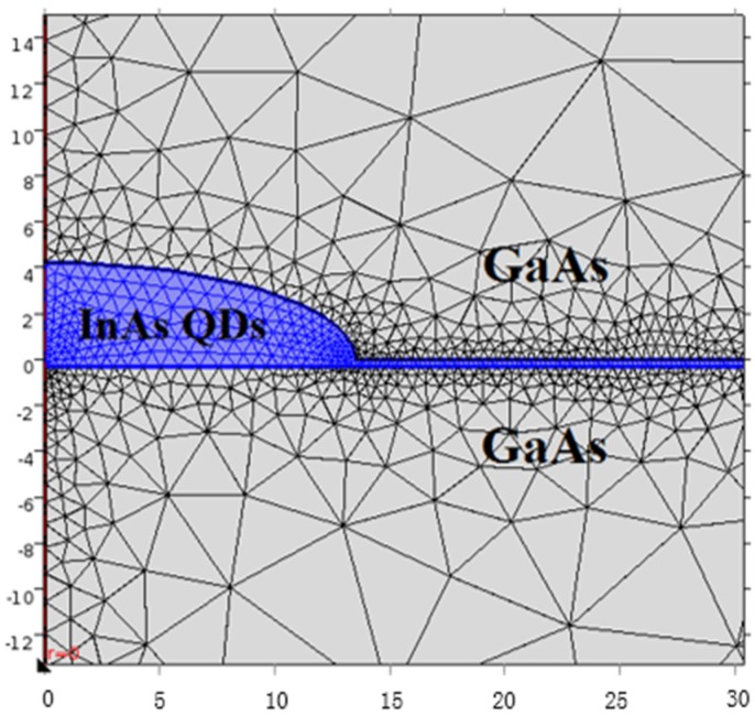
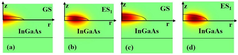
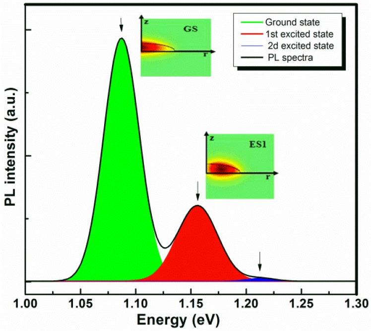
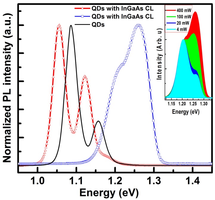
This work reports on theoretical and experimental investigation of the impact of InAs quantum dots (QDs) position with respect to InGaAs strain reducing layer (SRL). The investigated samples are grown by molecular beam epitaxy and characterized by photoluminescence spectroscopy (PL). The QDs optical transition energies have been calculated by solving the three dimensional Schrödinger equation using the finite element methods and taking into account the strain induced by the lattice mismatch. We have considered a lens shaped InAs QDs in a pure GaAs matrix and either with InGaAs strain reducing cap layer or underlying layer. The correlation between numerical calculation and PL measurements allowed us to track the mean buried QDs size evolution with respect to the surrounding matrix composition. The simulations reveal that the buried QDs' realistic size is less than that experimentally driven from atomic force microscopy observation. Furthermore, the average size is found to be slightly increased for InGaAs capped QDs and dramatically decreased for QDs with InGaAs under layer.

摘要

本工作报道了关于InAs量子点(QD)相对于InGaAs应变降低层(SRL)位置影响的理论和实验研究。所研究的样品通过分子束外延生长,并通过光致发光光谱(PL)进行表征。通过使用有限元方法求解三维薛定谔方程,并考虑晶格失配引起的应变,计算了量子点的光学跃迁能量。我们考虑了在纯GaAs基质中、带有InGaAs应变降低帽层或底层的透镜形状InAs量子点。数值计算与PL测量之间的相关性使我们能够追踪平均掩埋量子点尺寸相对于周围基质成分的演变。模拟结果表明,掩埋量子点的实际尺寸小于通过原子力显微镜观察实验得出的尺寸。此外,发现对于有InGaAs帽层的量子点,平均尺寸略有增加,而对于有InGaAs底层的量子点,平均尺寸则显著减小。

https://cdn.ncbi.nlm.nih.gov/pmc/blobs/6ce1/5455476/16573728e882/materials-08-04699-g004.jpg
https://cdn.ncbi.nlm.nih.gov/pmc/blobs/6ce1/5455476/f5652d2cb683/materials-08-04699-g001.jpg
https://cdn.ncbi.nlm.nih.gov/pmc/blobs/6ce1/5455476/f1b2dfb6b724/materials-08-04699-g002.jpg
https://cdn.ncbi.nlm.nih.gov/pmc/blobs/6ce1/5455476/9d5441fd9c0d/materials-08-04699-g003.jpg
https://cdn.ncbi.nlm.nih.gov/pmc/blobs/6ce1/5455476/16573728e882/materials-08-04699-g004.jpg

相似文献

1
Investigation of the InAs/GaAs Quantum Dots' Size: Dependence on the Strain Reducing Layer's Position.砷化铟/砷化镓量子点尺寸的研究:对应变降低层位置的依赖性。
Materials (Basel). 2015 Jul 24;8(8):4699-4709. doi: 10.3390/ma8084699.
2
Morphology and optical properties of single- and multi-layer InAs quantum dots.单层和多层砷化铟量子点的形态与光学性质
J Electron Microsc (Tokyo). 2010 Aug;59 Suppl 1:S149-54. doi: 10.1093/jmicro/dfq053. Epub 2010 Jun 24.
3
O-Band Emitting InAs Quantum Dots Grown By MOCVD On A 300 mm Ge-Buffered Si (001) Substrate.通过金属有机化学气相沉积(MOCVD)在300毫米锗缓冲硅(001)衬底上生长的发射O波段的砷化铟量子点
Nanomaterials (Basel). 2020 Dec 7;10(12):2450. doi: 10.3390/nano10122450.
4
Electronic and Optical Properties of InAs QDs Grown by MBE on InGaAs Metamorphic Buffer.分子束外延法在铟镓砷变质缓冲层上生长的砷化铟量子点的电学和光学性质
Materials (Basel). 2022 Jan 29;15(3):1071. doi: 10.3390/ma15031071.
5
Enhancing optical characteristics of InAs/InGaAsSb quantum dot structures with long-excited state emission at 1.31 μm.增强具有1.31μm长激发态发射的InAs/InGaAsSb量子点结构的光学特性。
Opt Express. 2014 Aug 11;22(16):18860-9. doi: 10.1364/OE.22.018860.
6
Long-wavelength emission InAs quantum dots grown on InGaAs metamorphic buffers.生长在InGaAs变质缓冲层上的长波长发射InAs量子点。
J Nanosci Nanotechnol. 2009 Feb;9(2):1333-6. doi: 10.1166/jnn.2009.c150.
7
Correlating Photoluminescence and Structural Properties of Uncapped and GaAs-Capped Epitaxial InGaAs Quantum Dots.未盖帽和砷化镓盖帽的外延铟镓砷量子点的光致发光与结构特性的关联
Sci Rep. 2018 May 14;8(1):7514. doi: 10.1038/s41598-018-25841-7.
8
Structure and composition profile of InAs/GaAs quantum dots capped by an InGaAs and InAlAs combination layer.由 InGaAs 和 InAlAs 组合层覆盖的 InAs/GaAs 量子点的结构和组成分布。
Nanotechnology. 2010 Jun 25;21(25):255705. doi: 10.1088/0957-4484/21/25/255705. Epub 2010 Jun 2.
9
Suppression of dislocations by Sb spray in the vicinity of InAs/GaAs quantum dots.通过 Sb 喷雾在 InAs/GaAs 量子点附近抑制位错。
Nanoscale Res Lett. 2014 May 30;9(1):278. doi: 10.1186/1556-276X-9-278. eCollection 2014.
10
Detecting Spatially Localized Exciton in Self-Organized InAs/InGaAs Quantum Dot Superlattices: a Way to Improve the Photovoltaic Efficiency.在自组织InAs/InGaAs量子点超晶格中检测空间局域激子:提高光伏效率的一种方法。
Nanoscale Res Lett. 2017 Dec;12(1):450. doi: 10.1186/s11671-017-2218-2. Epub 2017 Jul 11.

引用本文的文献

1
O-Band Emitting InAs Quantum Dots Grown By MOCVD On A 300 mm Ge-Buffered Si (001) Substrate.通过金属有机化学气相沉积(MOCVD)在300毫米锗缓冲硅(001)衬底上生长的发射O波段的砷化铟量子点
Nanomaterials (Basel). 2020 Dec 7;10(12):2450. doi: 10.3390/nano10122450.
2
Intersubband Optical Nonlinearity of GeSn Quantum Dots under Vertical Electric Field.垂直电场下GeSn量子点的子带间光学非线性
Micromachines (Basel). 2019 Apr 12;10(4):243. doi: 10.3390/mi10040243.
3
Linear and Nonlinear Intersubband Optical Properties of Direct Band Gap GeSn Quantum Dots.

本文引用的文献

1
Improved quantum dot stacking for intermediate band solar cells using strain compensation.利用应变补偿改进用于中间带太阳能电池的量子点堆叠。
Nanotechnology. 2014 Nov 7;25(44):445402. doi: 10.1088/0957-4484/25/44/445402. Epub 2014 Oct 16.
2
Intermediate-band dynamics of quantum dots solar cell in concentrator photovoltaic modules.聚光光伏模块中量子点太阳能电池的中间带动力学
Sci Rep. 2014 Apr 25;4:4792. doi: 10.1038/srep04792.
3
An entangled-light-emitting diode.纠缠发光二极管。
直接带隙GeSn量子点的线性和非线性子带间光学性质
Nanomaterials (Basel). 2019 Jan 19;9(1):124. doi: 10.3390/nano9010124.
4
Variation of the photoluminescence spectrum of InAs/GaAs heterostructures grown by ion-beam deposition.通过离子束沉积生长的InAs/GaAs异质结构的光致发光光谱变化
Beilstein J Nanotechnol. 2018 Nov 2;9:2794-2801. doi: 10.3762/bjnano.9.261. eCollection 2018.
5
Design of Strain-Engineered GeSn/GeSiSn Quantum Dots for Mid-IR Direct Bandgap Emission on Si Substrate.用于在硅衬底上实现中红外直接带隙发射的应变工程锗锡/锗硅锡量子点设计
Nanoscale Res Lett. 2018 Jun 7;13(1):172. doi: 10.1186/s11671-018-2587-1.
Nature. 2010 Jun 3;465(7298):594-7. doi: 10.1038/nature09078.