Department of Experimental Physics, Saarland University, Campus D2.2, 66123, Saarbrücken, Germany.
Institute of Micro and Nanomaterials, Ulm University, Albert-Einstein-Allee 47, 89081, Ulm, Germany.
Sci Rep. 2018 Jan 25;8(1):1592. doi: 10.1038/s41598-018-19588-4.
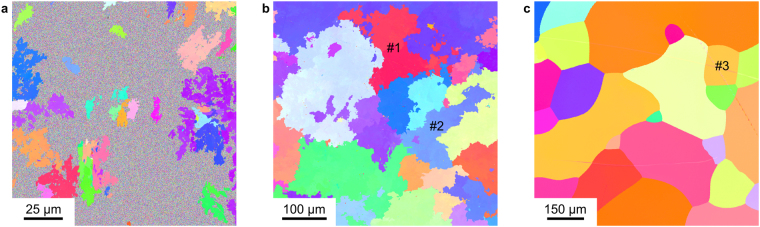
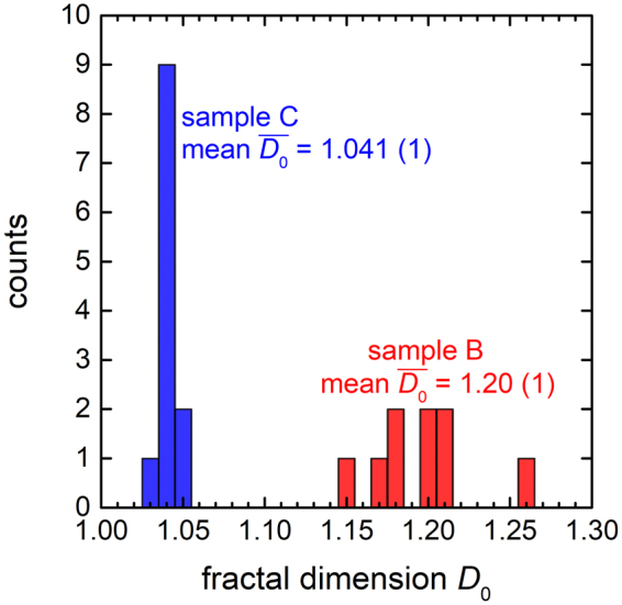
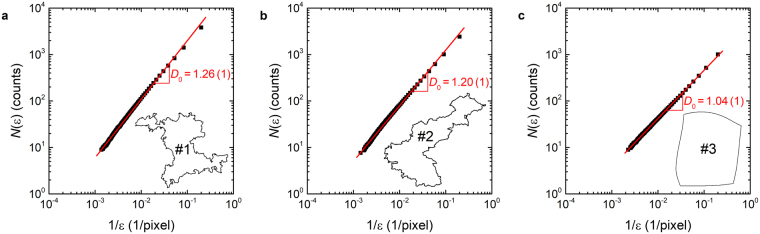
Modern engineered materials are composed of space-filling grains or domains separated by a network of interfaces or boundaries. Such polycrystalline microstructures have the capacity to coarsen through boundary migration. Grain growth theories account for the topology of grains and the connectivity of the boundary network in terms of the familiar Euclidian dimension and Euler's polyhedral formula, both of which are based on integer numbers. However, we recently discovered an unusual growth mode in a nanocrystalline Pd-Au alloy, in which grains develop complex, highly convoluted surface morphologies that are best described by a fractional dimension of ∼1.2 (extracted from the perimeters of grain cross sections). This fractal value is characteristic of a variety of domain growth scenarios-including explosive percolation, watersheds of random landscapes, and the migration of domain walls in a random field of pinning centers-which suggests that fractal grain boundary migration could be a manifestation of the same universal behavior.
现代工程材料由充满空间的晶粒或域组成,这些晶粒或域由界面或边界的网络隔开。这种多晶微观结构具有通过边界迁移粗化的能力。晶粒生长理论根据常见的欧几里得维度和欧拉多面体公式来解释晶粒的拓扑结构和边界网络的连通性,这两者都基于整数。然而,我们最近在纳米晶 Pd-Au 合金中发现了一种不寻常的生长模式,其中晶粒呈现出复杂的、高度曲折的表面形态,用分数维度(从晶粒截面的周长中提取)约 1.2 来描述最为合适。这个分形值是各种畴生长场景的特征,包括爆炸渗流、随机景观的分水岭以及在随机钉扎中心场中畴壁的迁移,这表明分形晶界迁移可能是同一普遍行为的表现。