Banerji Sourangsu, Sensale-Rodriguez Berardi
Department of Electrical and Computer Engineering, University of Utah, Salt Lake City, UT, 84112, USA.
Sci Rep. 2019 Apr 9;9(1):5801. doi: 10.1038/s41598-019-42243-5.
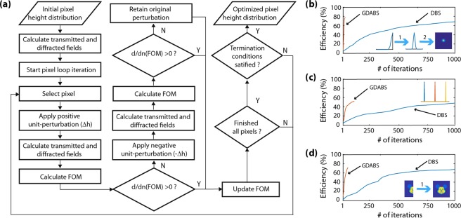
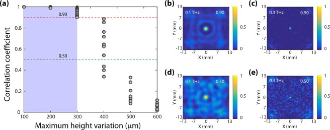
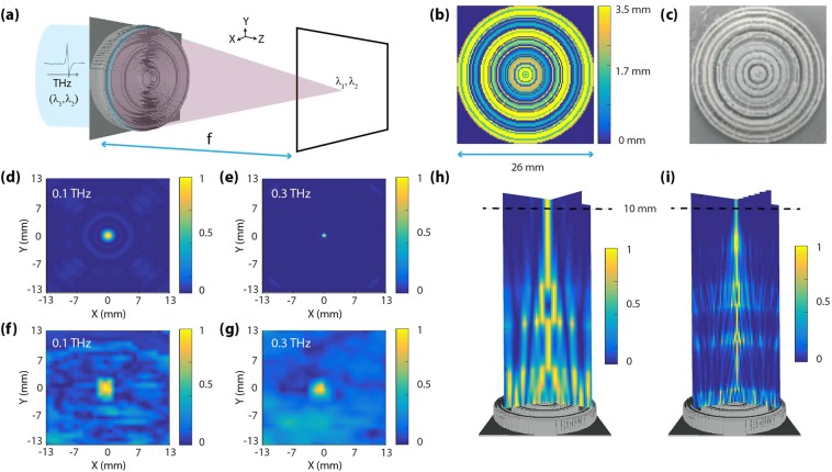
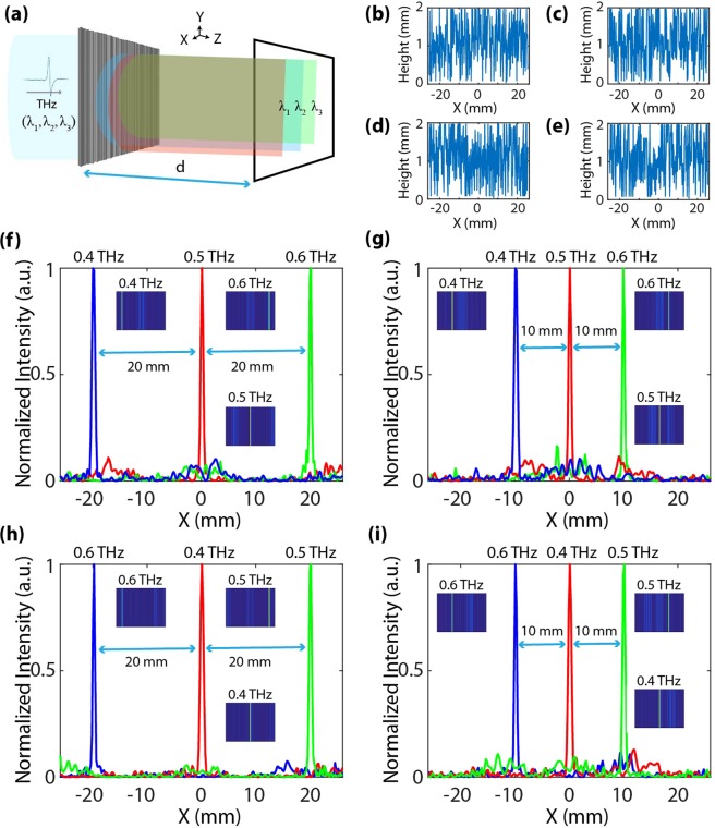
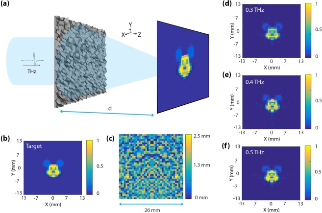
We demonstrate ultra-thin (1.5-3λ), fabrication-error tolerant efficient diffractive terahertz (THz) optical elements designed using a computer-aided optimization-based search algorithm. The basic operation of these components is modeled using scalar diffraction of electromagnetic waves through a pixelated multi-level 3D-printed polymer structure. Through the proposed design framework, we demonstrate the design of various ultrathin planar THz optical elements, namely (i) a high Numerical Aperture (N.A.), broadband aberration rectified spherical lens (0.1 THz-0.3 THz), (ii) a spectral splitter (0.3 THz-0.6 THz) and (iii) an on-axis broadband transmissive hologram (0.3 THz-0.5 THz). Such an all-dielectric computational design-based approach is advantageous against metallic or dielectric metasurfaces from the perspective that it incorporates all the inherent structural advantages associated with a scalar diffraction based approach, such as (i) ease of modeling, (ii) substrate-less facile manufacturing, (iii) planar geometry, (iv) high efficiency along with (v) broadband operation, (vi) area scalability and (vii) fabrication error-tolerance. With scalability and error tolerance being two major bottlenecks of previous design strategies. This work is therefore, a significant step towards the design of THz optical elements by bridging the gap between structural and computational design i.e. through a hybrid design-based approach enabling considerably less computational resources than the previous state of the art. Furthermore, the approach used herein can be expanded to a myriad of optical elements at any wavelength regime.
我们展示了使用基于计算机辅助优化的搜索算法设计的超薄(1.5 - 3λ)、容忍制造误差的高效衍射太赫兹(THz)光学元件。这些元件的基本操作是通过电磁波通过像素化多层3D打印聚合物结构的标量衍射进行建模的。通过所提出的设计框架,我们展示了各种超薄平面太赫兹光学元件的设计,即(i)高数值孔径(N.A.)、宽带像差校正球面透镜(0.1 THz - 0.3 THz),(ii)光谱分离器(0.3 THz - 0.6 THz)和(iii)同轴宽带透射全息图(0.3 THz - 0.5 THz)。这种基于全介质计算设计的方法相对于金属或介质超表面具有优势,因为它结合了基于标量衍射方法的所有固有结构优势,例如(i)易于建模,(ii)无基板的便捷制造,(iii)平面几何形状,(iv)高效率以及(v)宽带操作,(vi)面积可扩展性和(vii)制造误差容忍度。可扩展性和误差容忍度是先前设计策略的两个主要瓶颈。因此,这项工作是朝着太赫兹光学元件设计迈出的重要一步,通过弥合结构设计和计算设计之间的差距,即通过基于混合设计的方法,与先前的技术水平相比,所需的计算资源大大减少。此外,本文中使用的方法可以扩展到任何波长范围的众多光学元件。