• 文献检索
  • 文档翻译
  • 深度研究
  • 学术资讯
  • Suppr Zotero 插件Zotero 插件
  • 邀请有礼
  • 套餐&价格
  • 历史记录
应用&插件
Suppr Zotero 插件Zotero 插件浏览器插件Mac 客户端Windows 客户端微信小程序
定价
高级版会员购买积分包购买API积分包
服务
文献检索文档翻译深度研究API 文档MCP 服务
关于我们
关于 Suppr公司介绍联系我们用户协议隐私条款
关注我们

Suppr 超能文献

核心技术专利:CN118964589B侵权必究
粤ICP备2023148730 号-1Suppr @ 2026

文献检索

告别复杂PubMed语法,用中文像聊天一样搜索,搜遍4000万医学文献。AI智能推荐,让科研检索更轻松。

立即免费搜索

文件翻译

保留排版,准确专业,支持PDF/Word/PPT等文件格式,支持 12+语言互译。

免费翻译文档

深度研究

AI帮你快速写综述,25分钟生成高质量综述,智能提取关键信息,辅助科研写作。

立即免费体验

使用超薄铂催化剂通过PECVD在GaN LED外延片上生长用于透明电极应用的无转移类石墨烯薄膜。

Transfer-Free Graphene-Like Thin Films on GaN LED Epiwafers Grown by PECVD Using an Ultrathin Pt Catalyst for Transparent Electrode Applications.

作者信息

Xiong Fangzhu, Guo Weiling, Feng Shiwei, Li Xuan, Du Zaifa, Wang Le, Deng Jun, Sun Jie

机构信息

Key Laboratory of Optoelectronics Technology, College of Microelectronics, Beijing University of Technology, Beijing 100124, China.

Quantum Device Physics Laboratory, Department of Microtechnology and Nanoscience, Chalmers University of Technology, 41296 Gothenburg, Sweden.

出版信息

Materials (Basel). 2019 Oct 28;12(21):3533. doi: 10.3390/ma12213533.

DOI:10.3390/ma12213533
PMID:31661874
原文链接:https://pmc.ncbi.nlm.nih.gov/articles/PMC6862194/
Abstract

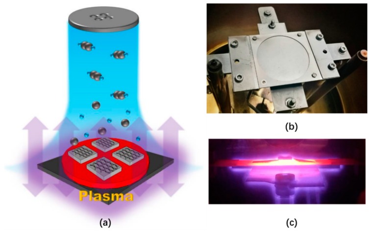
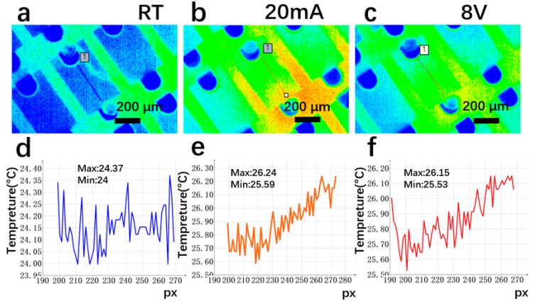
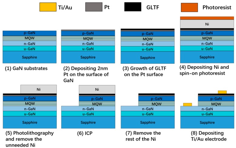
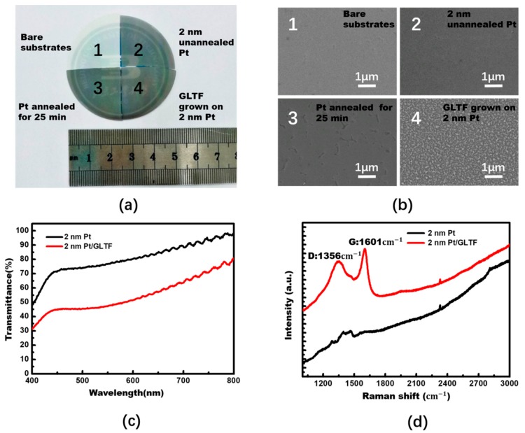
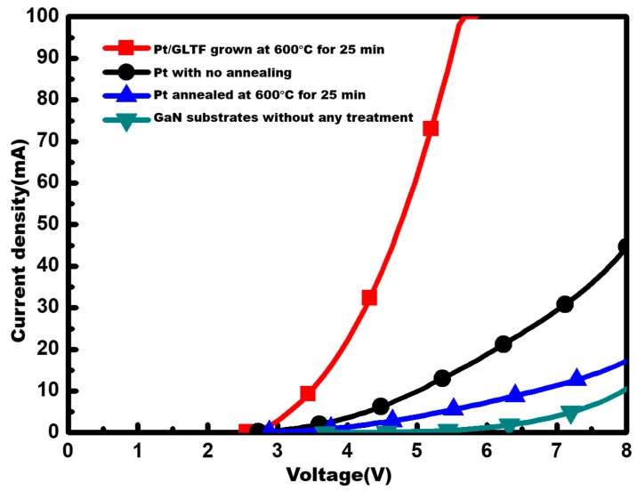
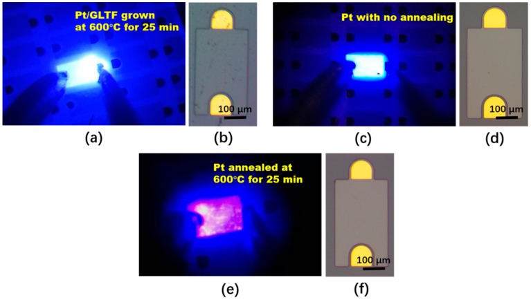
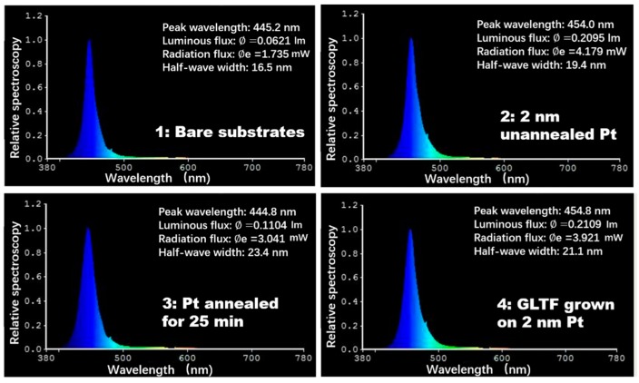
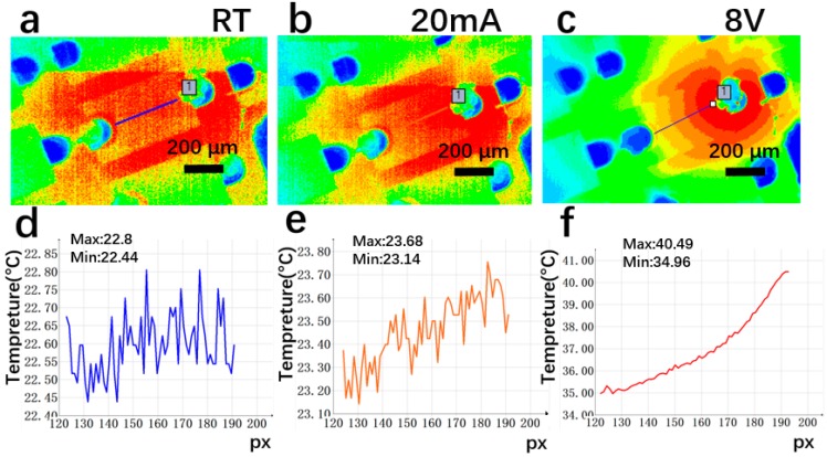
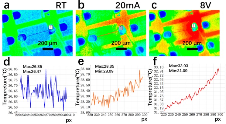
In this work, we grew transfer-free graphene-like thin films (GLTFs) directly on gallium nitride (GaN)/sapphire light-emitting diode (LED) substrates. Their electrical, optical and thermal properties were studied for transparent electrode applications. Ultrathin platinum (2 nm) was used as the catalyst in the plasma-enhanced chemical vapor deposition (PECVD). The growth parameters were adjusted such that the high temperature exposure of GaN wafers was reduced to its minimum (deposition temperature as low as 600 °C) to ensure the intactness of GaN epilayers. In a comparison study of the Pt-GLTF GaN LED devices and Pt-only LED devices, the former was found to be superior in most aspects, including surface sheet resistance, power consumption, and temperature distribution, but not in optical transmission. This confirmed that the as-developed GLTF-based transparent electrodes had good current spreading, current injection and thermal spreading functionalities. Most importantly, the technique presented herein does not involve any material transfer, rendering a scalable, controllable, reproducible and semiconductor industry-compatible solution for transparent electrodes in GaN-based optoelectronic devices.

摘要

在这项工作中,我们直接在氮化镓(GaN)/蓝宝石发光二极管(LED)衬底上生长了无转移的类石墨烯薄膜(GLTFs)。研究了它们用于透明电极应用时的电学、光学和热学性质。在等离子体增强化学气相沉积(PECVD)中,使用超薄铂(2纳米)作为催化剂。调整生长参数,使GaN晶片的高温暴露降至最低(沉积温度低至600°C),以确保GaN外延层的完整性。在对基于Pt-GLTF的GaN LED器件和仅含Pt的LED器件的比较研究中,发现前者在大多数方面表现更优,包括表面薄层电阻、功耗和温度分布,但在光传输方面并非如此。这证实了所开发的基于GLTF的透明电极具有良好的电流扩展、电流注入和热扩散功能。最重要的是,本文提出的技术不涉及任何材料转移,为基于GaN的光电器件中的透明电极提供了一种可扩展、可控、可重复且与半导体工业兼容的解决方案。

https://cdn.ncbi.nlm.nih.gov/pmc/blobs/324d/6862194/6230fc92ad3e/materials-12-03533-g010.jpg
https://cdn.ncbi.nlm.nih.gov/pmc/blobs/324d/6862194/4767fe2c651f/materials-12-03533-g001.jpg
https://cdn.ncbi.nlm.nih.gov/pmc/blobs/324d/6862194/d5d5db68d4a4/materials-12-03533-g002.jpg
https://cdn.ncbi.nlm.nih.gov/pmc/blobs/324d/6862194/132ef75c2fde/materials-12-03533-g003.jpg
https://cdn.ncbi.nlm.nih.gov/pmc/blobs/324d/6862194/7af372c1167e/materials-12-03533-g004.jpg
https://cdn.ncbi.nlm.nih.gov/pmc/blobs/324d/6862194/2777c76bfea3/materials-12-03533-g005.jpg
https://cdn.ncbi.nlm.nih.gov/pmc/blobs/324d/6862194/e7f90799ce3a/materials-12-03533-g006.jpg
https://cdn.ncbi.nlm.nih.gov/pmc/blobs/324d/6862194/fc1b7b035d70/materials-12-03533-g007.jpg
https://cdn.ncbi.nlm.nih.gov/pmc/blobs/324d/6862194/9162858ea26a/materials-12-03533-g008.jpg
https://cdn.ncbi.nlm.nih.gov/pmc/blobs/324d/6862194/fef134d6ba70/materials-12-03533-g009.jpg
https://cdn.ncbi.nlm.nih.gov/pmc/blobs/324d/6862194/6230fc92ad3e/materials-12-03533-g010.jpg

相似文献

1
Transfer-Free Graphene-Like Thin Films on GaN LED Epiwafers Grown by PECVD Using an Ultrathin Pt Catalyst for Transparent Electrode Applications.使用超薄铂催化剂通过PECVD在GaN LED外延片上生长用于透明电极应用的无转移类石墨烯薄膜。
Materials (Basel). 2019 Oct 28;12(21):3533. doi: 10.3390/ma12213533.
2
Graphene as a Transparent Conductive Electrode in GaN-Based LEDs.石墨烯作为基于氮化镓发光二极管中的透明导电电极。
Materials (Basel). 2022 Mar 16;15(6):2203. doi: 10.3390/ma15062203.
3
Graphene transparent electrode for enhanced optical power and thermal stability in GaN light-emitting diodes.用于提高 GaN 发光二极管的光功率和热稳定性的石墨烯透明电极。
Nanotechnology. 2013 Feb 22;24(7):075202. doi: 10.1088/0957-4484/24/7/075202. Epub 2013 Jan 28.
4
GaN/AlGaN Nanocolumn Ultraviolet Light-Emitting Diode Using Double-Layer Graphene as Substrate and Transparent Electrode.基于双层石墨烯的 GaN/AlGaN 纳米柱紫外发光二极管及其透明电极
Nano Lett. 2019 Mar 13;19(3):1649-1658. doi: 10.1021/acs.nanolett.8b04607. Epub 2019 Feb 6.
5
High-Brightness Blue Light-Emitting Diodes Enabled by a Directly Grown Graphene Buffer Layer.直接生长的石墨烯缓冲层实现高光亮度蓝光发光二极管。
Adv Mater. 2018 Jul;30(30):e1801608. doi: 10.1002/adma.201801608. Epub 2018 Jun 8.
6
Transferable GaN layers grown on ZnO-coated graphene layers for optoelectronic devices.在 ZnO 涂层石墨烯层上生长的可转移 GaN 层,用于光电器件。
Science. 2010 Oct 29;330(6004):655-7. doi: 10.1126/science.1195403.
7
Large-scale patterned multi-layer graphene films as transparent conducting electrodes for GaN light-emitting diodes.大面积图案化多层石墨烯薄膜作为 GaN 发光二极管的透明导电电极。
Nanotechnology. 2010 Apr 30;21(17):175201. doi: 10.1088/0957-4484/21/17/175201. Epub 2010 Apr 6.
8
Hybrid Tunnel Junction-Graphene Transparent Conductive Electrodes for Nitride Lateral Light Emitting Diodes.用于氮化物横向发光二极管的混合隧道结-石墨烯透明导电电极
ACS Appl Mater Interfaces. 2016 Jan 20;8(2):1176-83. doi: 10.1021/acsami.5b09419. Epub 2016 Jan 7.
9
Monolithic Integrated Device of GaN Micro-LED with Graphene Transparent Electrode and Graphene Active-Matrix Driving Transistor.具有石墨烯透明电极和石墨烯有源矩阵驱动晶体管的氮化镓微发光二极管单片集成器件
Materials (Basel). 2019 Jan 30;12(3):428. doi: 10.3390/ma12030428.
10
Opposite Behavior of Multilayer Graphene/ Indium-Tin-Oxide -Electrode for Gallium Nitride Based-Light Emitting Diodes Depending on Thickness of Indium-Tin-Oxide Layer.基于氮化镓发光二极管的多层石墨烯/氧化铟锡电极的相反行为取决于氧化铟锡层的厚度。
J Nanosci Nanotechnol. 2018 Sep 1;18(9):6106-6111. doi: 10.1166/jnn.2018.15603.

引用本文的文献

1
Comparative Research of GaN Growth Mechanisms on Patterned Sapphire Substrates with Sputtered AlON Nucleation Layers.具有溅射AlON成核层的图案化蓝宝石衬底上GaN生长机制的比较研究。
Materials (Basel). 2020 Sep 5;13(18):3933. doi: 10.3390/ma13183933.
2
High Quality Graphene Thin Films Synthesized by Glow Discharge Method in A Chemical Vapor Deposition System Using Solid Carbon Source.在使用固体碳源的化学气相沉积系统中通过辉光放电法合成的高质量石墨烯薄膜。
Materials (Basel). 2020 Apr 26;13(9):2026. doi: 10.3390/ma13092026.

本文引用的文献

1
Layer number and stacking sequence imaging of few-layer graphene by transmission electron microscopy.利用透射电子显微镜对少层石墨烯的层数和堆叠序列成像。
Nano Lett. 2012 Sep 12;12(9):4635-41. doi: 10.1021/nl301932v. Epub 2012 Aug 15.
2
Repeated growth and bubbling transfer of graphene with millimetre-size single-crystal grains using platinum.采用铂实现毫米级单晶颗粒石墨烯的重复生长和鼓泡转移。
Nat Commun. 2012 Feb 28;3:699. doi: 10.1038/ncomms1702.
3
Transparent conductive graphene electrode in GaN-based ultra-violet light emitting diodes.
基于氮化镓的紫外发光二极管中的透明导电石墨烯电极。
Opt Express. 2010 Oct 25;18(22):23030-4. doi: 10.1364/OE.18.023030.
4
Large-scale patterned multi-layer graphene films as transparent conducting electrodes for GaN light-emitting diodes.大面积图案化多层石墨烯薄膜作为 GaN 发光二极管的透明导电电极。
Nanotechnology. 2010 Apr 30;21(17):175201. doi: 10.1088/0957-4484/21/17/175201. Epub 2010 Apr 6.
5
Electric field effect in atomically thin carbon films.原子级薄碳膜中的电场效应。
Science. 2004 Oct 22;306(5696):666-9. doi: 10.1126/science.1102896.
6
The roles of structural imperfections in InGaN-based blue light-emitting diodes and laser diodes.结构缺陷在基于氮化铟镓的蓝光发光二极管和激光二极管中的作用。
Science. 1998 Aug 14;281(5379):955-61. doi: 10.1126/science.281.5379.956.