• 文献检索
  • 文档翻译
  • 深度研究
  • 学术资讯
  • Suppr Zotero 插件Zotero 插件
  • 邀请有礼
  • 套餐&价格
  • 历史记录
应用&插件
Suppr Zotero 插件Zotero 插件浏览器插件Mac 客户端Windows 客户端微信小程序
定价
高级版会员购买积分包购买API积分包
服务
文献检索文档翻译深度研究API 文档MCP 服务
关于我们
关于 Suppr公司介绍联系我们用户协议隐私条款
关注我们

Suppr 超能文献

核心技术专利:CN118964589B侵权必究
粤ICP备2023148730 号-1Suppr @ 2026

文献检索

告别复杂PubMed语法,用中文像聊天一样搜索,搜遍4000万医学文献。AI智能推荐,让科研检索更轻松。

立即免费搜索

文件翻译

保留排版,准确专业,支持PDF/Word/PPT等文件格式,支持 12+语言互译。

免费翻译文档

深度研究

AI帮你快速写综述,25分钟生成高质量综述,智能提取关键信息,辅助科研写作。

立即免费体验

用于近红外烧结的银纳米颗粒喷墨油墨的层形态与油墨兼容性

Layer Morphology and Ink Compatibility of Silver Nanoparticle Inkjet Inks for Near-Infrared Sintering.

作者信息

Reenaers Dieter, Marchal Wouter, Biesmans Ianto, Nivelle Philippe, D'Haen Jan, Deferme Wim

机构信息

Institute for Materials Research (IMO), Universiteit Hasselt, Wetenschapspark 1, B-3590 Diepenbeek, Belgium.

IMEC vzw, Division IMOMEC, Wetenschapspark 1, B-3590 Diepenbeek, Belgium.

出版信息

Nanomaterials (Basel). 2020 May 7;10(5):892. doi: 10.3390/nano10050892.

DOI:10.3390/nano10050892
PMID:32392730
原文链接:https://pmc.ncbi.nlm.nih.gov/articles/PMC7279230/
Abstract

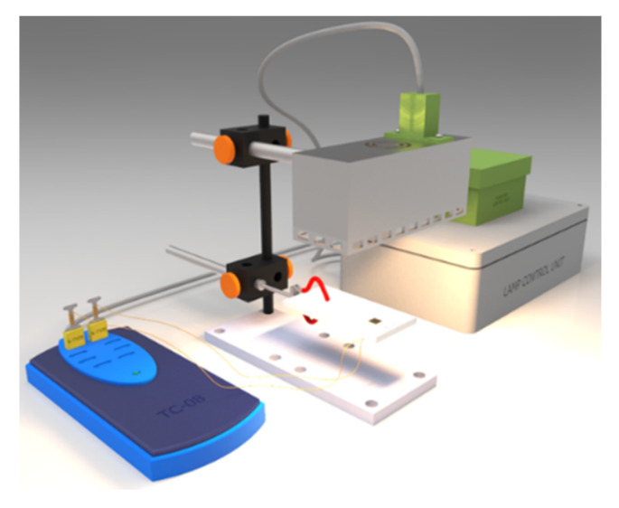
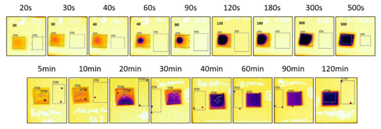
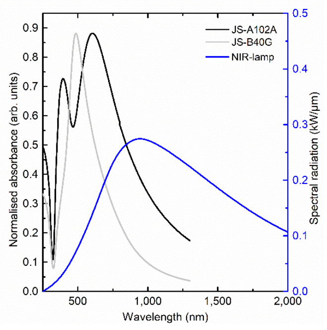
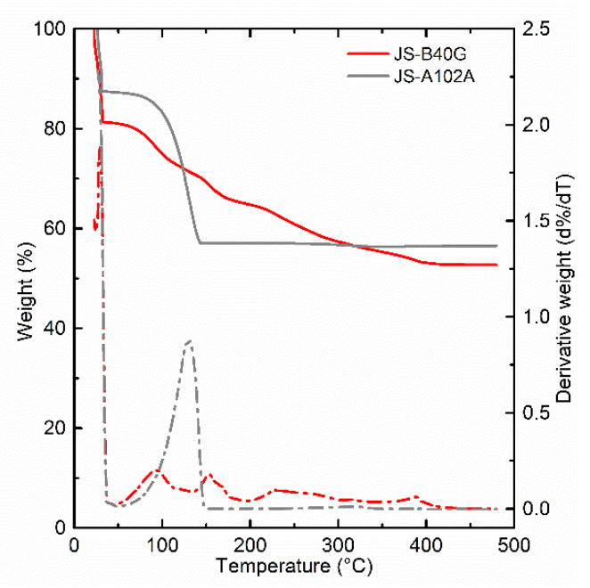
The field of printed electronics is rapidly evolving, producing low cost applications with enhanced performances with transparent, stretchable properties and higher reliability. Due to the versatility of printed electronics, industry can consider the implementation of electronics in a way which was never possible before. However, a post-processing step to achieve conductive structures-known as sintering-limits the production ease and speed of printed electronics. This study addresses the issues related to fast sintering without scarifying important properties such as conductivity and surface roughness. A drop-on-demand inkjet printer is employed to deposit silver nanoparticle-based inks. The post-processing time of these inks is reduced by replacing the conventional oven sintering procedure with the state-of-the-art method, named near-infrared sintering. By doing so, the post-processing time shortens from 30-60 min to 6-8 s. Furthermore, the maximum substrate temperature during sintering is reduced from 200 °C to 120 °C. Based on the results of this study, one can conclude that near-infrared sintering is a ready-to-industrialize post-processing method for the production of printed electronics, capable of sintering inks at high speed, low temperature and with low complexity. Furthermore, it becomes clear that ink optimization plays an important role in processing inkjet printable inks, especially after being near-infrared sintered.

摘要

印刷电子领域正在迅速发展,能够生产出具有增强性能的低成本应用产品,这些产品具有透明、可拉伸的特性以及更高的可靠性。由于印刷电子的多功能性,工业界可以以前所未有的方式考虑电子器件的应用。然而,实现导电结构的后处理步骤(即烧结)限制了印刷电子的生产便利性和速度。本研究解决了与快速烧结相关的问题,同时又不牺牲诸如导电性和表面粗糙度等重要性能。采用按需滴液式喷墨打印机来沉积基于银纳米颗粒的墨水。通过用名为近红外烧结的先进方法取代传统的烘箱烧结程序,这些墨水的后处理时间得以缩短。这样一来,后处理时间从30 - 60分钟缩短至6 - 8秒。此外,烧结过程中的最高基板温度从200°C降至120°C。基于本研究的结果,可以得出结论,近红外烧结是一种可直接工业化的印刷电子生产后处理方法,能够在高速、低温且低复杂度的条件下烧结墨水。此外,很明显墨水优化在处理喷墨可打印墨水方面起着重要作用,尤其是在经过近红外烧结之后。

https://cdn.ncbi.nlm.nih.gov/pmc/blobs/9d77/7279230/ed46c7cefe2f/nanomaterials-10-00892-g008.jpg
https://cdn.ncbi.nlm.nih.gov/pmc/blobs/9d77/7279230/fb82cf88a7e0/nanomaterials-10-00892-g001.jpg
https://cdn.ncbi.nlm.nih.gov/pmc/blobs/9d77/7279230/a1ddf2bf3d9e/nanomaterials-10-00892-g002.jpg
https://cdn.ncbi.nlm.nih.gov/pmc/blobs/9d77/7279230/ccf355706c34/nanomaterials-10-00892-g003.jpg
https://cdn.ncbi.nlm.nih.gov/pmc/blobs/9d77/7279230/023ccfbdedcc/nanomaterials-10-00892-g005.jpg
https://cdn.ncbi.nlm.nih.gov/pmc/blobs/9d77/7279230/3de746ef140c/nanomaterials-10-00892-g006.jpg
https://cdn.ncbi.nlm.nih.gov/pmc/blobs/9d77/7279230/b1c037969bd9/nanomaterials-10-00892-g007.jpg
https://cdn.ncbi.nlm.nih.gov/pmc/blobs/9d77/7279230/ed46c7cefe2f/nanomaterials-10-00892-g008.jpg

相似文献

1
Layer Morphology and Ink Compatibility of Silver Nanoparticle Inkjet Inks for Near-Infrared Sintering.用于近红外烧结的银纳米颗粒喷墨油墨的层形态与油墨兼容性
Nanomaterials (Basel). 2020 May 7;10(5):892. doi: 10.3390/nano10050892.
2
Silver Nanoparticles Based Ink with Moderate Sintering in Flexible and Printed Electronics.基于银纳米粒子的油墨具有适度的烧结性,适用于柔性和印刷电子产品。
Int J Mol Sci. 2019 Apr 29;20(9):2124. doi: 10.3390/ijms20092124.
3
Systematic Investigation of Novel, Controlled Low-Temperature Sintering Processes for Inkjet Printed Silver Nanoparticle Ink.用于喷墨打印银纳米颗粒墨水的新型可控低温烧结工艺的系统研究。
Small. 2024 May;20(21):e2306865. doi: 10.1002/smll.202306865. Epub 2023 Dec 21.
4
Robust Design of a Particle-Free Silver-Organo-Complex Ink with High Conductivity and Inkjet Stability for Flexible Electronics.用于柔性电子器件的具有高导电性和喷墨稳定性的无颗粒银-有机络合物墨水的稳健设计。
ACS Appl Mater Interfaces. 2016 Jan 13;8(1):177-86. doi: 10.1021/acsami.5b08125. Epub 2015 Dec 29.
5
An Approach to a Silver Conductive Ink for Inkjet Printer Technology.一种适用于喷墨打印机技术的银导电油墨的研究方法。
Polymers (Basel). 2024 Jun 18;16(12):1731. doi: 10.3390/polym16121731.
6
Low-Thermal-Budget Photonic Processing of Highly Conductive Cu Interconnects Based on CuO Nanoinks: Potential for Flexible Printed Electronics.基于 CuO 纳米墨水的高热预算光子处理高导电性 Cu 互连:用于柔性印刷电子的潜力。
ACS Appl Mater Interfaces. 2016 Jan 27;8(3):2441-8. doi: 10.1021/acsami.5b12156. Epub 2016 Jan 12.
7
Inkjet Printing of Polyacrylic Acid-Coated Silver Nanoparticle Ink onto Paper with Sub-100 Micron Pixel Size.将聚丙烯酸包覆的银纳米颗粒油墨以小于100微米的像素尺寸喷墨打印到纸张上。
Materials (Basel). 2019 Jul 15;12(14):2277. doi: 10.3390/ma12142277.
8
Ohmic contact formation for inkjet-printed nanoparticle copper inks on highly doped GaAs.高掺杂砷化镓上喷墨打印纳米颗粒铜油墨的欧姆接触形成
Nanotechnology. 2021 Mar 12;32(22). doi: 10.1088/1361-6528/abe902.
9
Sintering Inhibition of Silver Nanoparticle Films via AgCl Nanocrystal Formation.通过氯化银纳米晶体形成抑制银纳米颗粒薄膜的烧结
Nanomaterials (Basel). 2017 Aug 17;7(8):224. doi: 10.3390/nano7080224.
10
Fast near infrared sintering of silver nanoparticle ink and applications for flexible hybrid circuits.银纳米颗粒墨水的快速近红外烧结及其在柔性混合电路中的应用。
RSC Adv. 2018 Aug 28;8(53):30215-30222. doi: 10.1039/c8ra04468f. eCollection 2018 Aug 24.

引用本文的文献

1
Developing Screen-Printing Processes for Silver Electrodes Towards All-Solution Coating Processes for Solar Cells.开发用于银电极的丝网印刷工艺,以实现太阳能电池的全溶液涂布工艺。
Polymers (Basel). 2024 Oct 27;16(21):3012. doi: 10.3390/polym16213012.
2
Wound-Dressing-Based Antenna Inkjet-Printed Using Nanosilver Ink for Wireless Medical Monitoring.基于伤口敷料的天线,采用纳米银墨水进行喷墨打印用于无线医疗监测。
Micromachines (Basel). 2022 Sep 12;13(9):1510. doi: 10.3390/mi13091510.
3
Screen Printed Antennas on Fiber-Based Substrates for Sustainable HF RFID Assisted E-Fulfilment Smart Packaging.

本文引用的文献

1
Understanding the Importance of Cu(I) Intermediates in Self-Reducing Molecular Inks for Flexible Electronics.理解Cu(I)中间体在用于柔性电子器件的自还原分子油墨中的重要性。
Inorg Chem. 2018 Dec 17;57(24):15205-15215. doi: 10.1021/acs.inorgchem.8b02493. Epub 2018 Nov 28.
2
Direct observation of aggregative nanoparticle growth: kinetic modeling of the size distribution and growth rate.直接观察聚集纳米颗粒的生长:尺寸分布和生长速率的动力学建模。
Nano Lett. 2014 Jan 8;14(1):373-8. doi: 10.1021/nl4043328. Epub 2013 Dec 12.
3
Sintering of catalytic nanoparticles: particle migration or Ostwald ripening?
基于纤维基材的丝网印刷天线用于可持续高频射频识别辅助电子履行智能包装
Materials (Basel). 2021 Sep 23;14(19):5500. doi: 10.3390/ma14195500.
4
Heat Scanning for the Fabrication of Conductive Fibers.用于制造导电纤维的热扫描
Polymers (Basel). 2021 Apr 26;13(9):1405. doi: 10.3390/polym13091405.
催化纳米粒子的烧结:颗粒迁移还是奥斯特瓦尔德熟化?
Acc Chem Res. 2013 Aug 20;46(8):1720-30. doi: 10.1021/ar3002427. Epub 2013 May 1.
4
Roll-to-roll compatible sintering of inkjet printed features by photonic and microwave exposure: from non-conductive ink to 40% bulk silver conductivity in less than 15 seconds.通过光子和微波曝光实现喷墨打印特征的卷对卷兼容烧结:在不到15秒的时间内从非导电油墨转变为具有40%体银导电性。
Adv Mater. 2012 May 15;24(19):2620-5. doi: 10.1002/adma.201104417. Epub 2012 Apr 10.
5
Inkjet-printed graphene electronics.喷墨打印石墨烯电子器件。
ACS Nano. 2012 Apr 24;6(4):2992-3006. doi: 10.1021/nn2044609. Epub 2012 Mar 26.
6
Synthesis of monodisperse silver nanoparticles for ink-jet printed flexible electronics.用于喷墨打印柔性电子的单分散银纳米粒子的合成。
Nanotechnology. 2011 Oct 21;22(42):425601. doi: 10.1088/0957-4484/22/42/425601. Epub 2011 Sep 22.