Kolasinski Kurt W
Department of Chemistry, West Chester University, West Chester, PA 19383, USA.
Micromachines (Basel). 2021 Jun 30;12(7):776. doi: 10.3390/mi12070776.
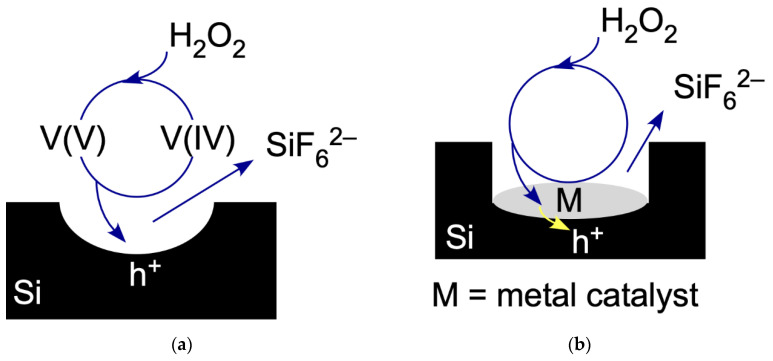
Electroless etching of semiconductors has been elevated to an advanced micromachining process by the addition of a structured metal catalyst. Patterning of the catalyst by lithographic techniques facilitated the patterning of crystalline and polycrystalline wafer substrates. Galvanic deposition of metals on semiconductors has a natural tendency to produce nanoparticles rather than flat uniform films. This characteristic makes possible the etching of wafers and particles with arbitrary shape and size. While it has been widely recognized that spontaneous deposition of metal nanoparticles can be used in connection with etching to porosify wafers, it is also possible to produced nanostructured powders. Metal-assisted catalytic etching (MACE) can be controlled to produce (1) etch track pores with shapes and sizes closely related to the shape and size of the metal nanoparticle, (2) hierarchically porosified substrates exhibiting combinations of large etch track pores and mesopores, and (3) nanowires with either solid or mesoporous cores. This review discussed the mechanisms of porosification, processing advances, and the properties of the etch product with special emphasis on the etching of silicon powders.
通过添加结构化金属催化剂,半导体的无电镀蚀刻已提升为一种先进的微加工工艺。通过光刻技术对催化剂进行图案化,有助于对晶体和多晶硅晶圆基板进行图案化。金属在半导体上的电沉积自然倾向于产生纳米颗粒而不是平整均匀的薄膜。这一特性使得蚀刻任意形状和尺寸的晶圆和颗粒成为可能。虽然人们普遍认识到金属纳米颗粒的自发沉积可与蚀刻结合使用以使晶圆形成多孔结构,但也有可能生产出纳米结构粉末。金属辅助催化蚀刻(MACE)可以控制以产生:(1)蚀刻轨迹孔,其形状和尺寸与金属纳米颗粒的形状和尺寸密切相关;(2)具有大蚀刻轨迹孔和中孔组合的分级多孔基板;以及(3)具有实心或中孔芯的纳米线。本综述讨论了多孔化机制、工艺进展以及蚀刻产物的特性,特别强调了硅粉的蚀刻。