Chen Meng-Hsin, Yen Cheng-Wei, Guo Chia-Chun, Su Vin-Cent, Kuan Chieh-Hsiung, Lin Hoang Yan
Department of Electrical Engineering and Graduate Institute of Photonics and Optoelectronics, National Taiwan University, Taipei, 10617, Taiwan.
Department of Electrical Engineering and Graduate Institute of Electronics Engineering, National Taiwan University, Taipei, 10617, Taiwan.
Sci Rep. 2021 Jul 15;11(1):14541. doi: 10.1038/s41598-021-94176-7.
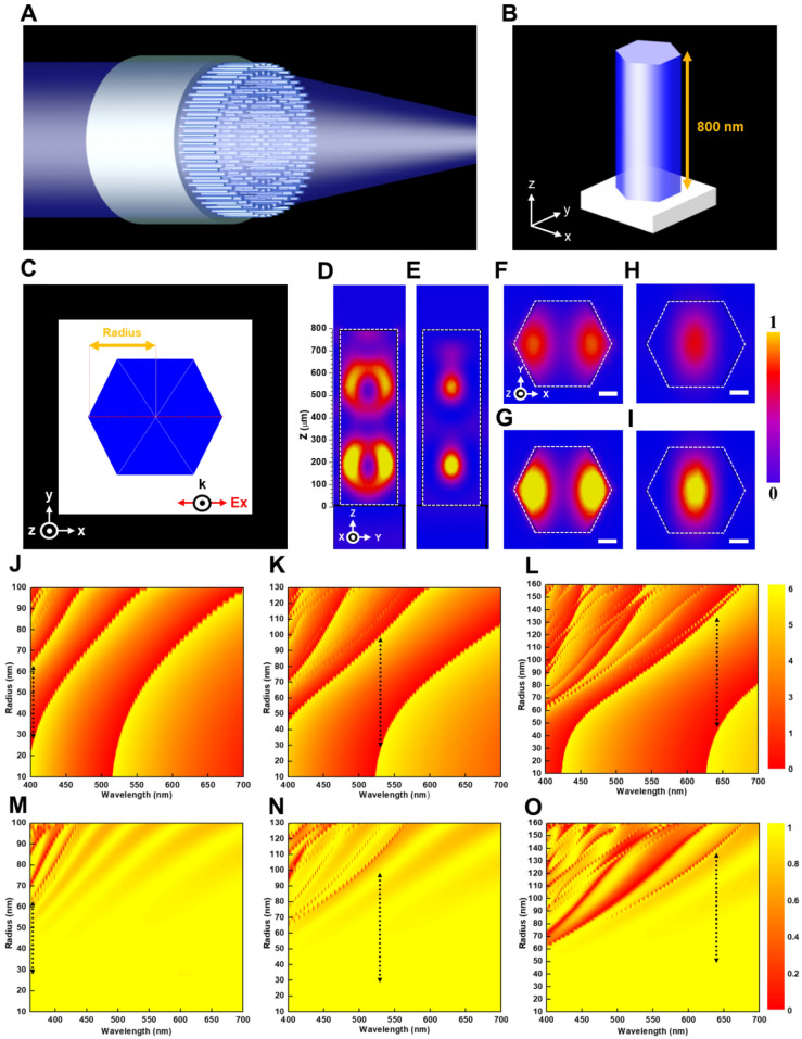
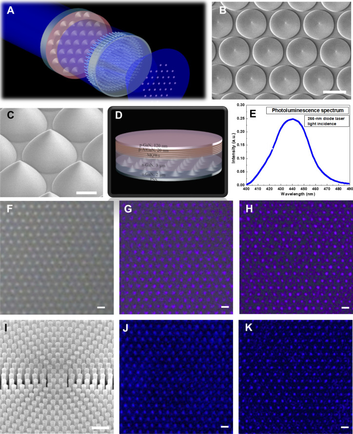
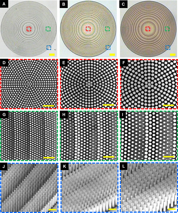
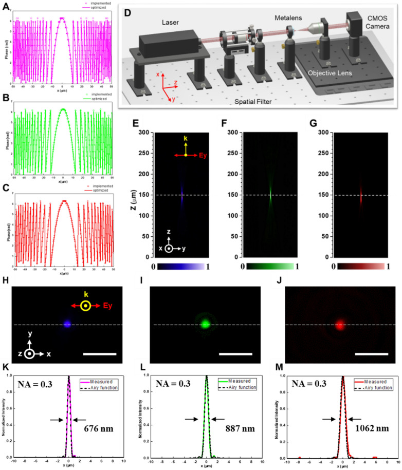
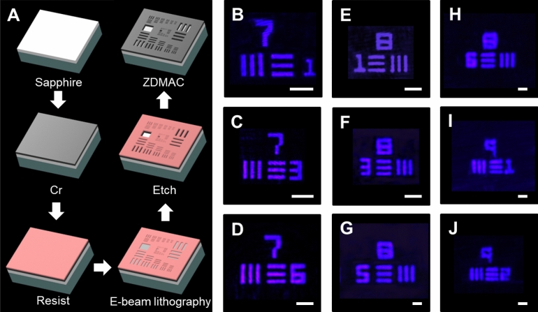
The growth of wide-bandgap materials on patterned substrates has revolutionized the means with which we can improve the light output power of gallium nitride (GaN) light-emitting diodes (LEDs). Conventional patterned structure inspection usually relies on an expensive vacuum-system-required scanning electron microscope (SEM) or optical microscope (OM) with bulky objectives. On the other hand, ultra-thin metasurfaces have been widely used in widespread applications, especially for converging lenses. In this study, we propose newly developed, highly efficient hexagon-resonated elements (HREs) combined with gingerly selected subwavelength periods of the elements for the construction of polarization-insensitive metalenses of high performance. Also, the well-developed fabrication techniques have been employed to realize the high-aspect-ratio metalenses working at three distinct wavelengths of 405, 532, and 633 nm with respective diffraction-limited focusing efficiencies of 93%, 86%, and 92%. The 1951 United States Air Force (USAF) test chart has been chosen to characterize the imaging capability. All of the images formed by the 405-nm-designed metalens show exceptional clear line features, and the smallest resolvable features are lines with widths of 870 nm. To perform the inspection capacity for patterned substrates, for the proof of concept, a commercially available patterned sapphire substrate (PSS) for the growth of the GaN LEDs has been opted and carefully examined by the high-resolution SEM system. With the appropriately chosen metalenses at the desired wavelength, the summits of structures in the PSS can be clearly observed in the images. The PSS imaging qualities taken by the ultra-thin and light-weight metalenses with a numerical aperture (NA) of 0.3 are comparable to those seen by an objective with the NA of 0.4. This work can pioneer semiconductor manufacturing to choose the polarization-insensitive GaN metalenses to inspect the patterned structures instead of using the SEM or the bulky and heavy conventional objectives.
在图案化衬底上生长宽带隙材料,彻底改变了我们提高氮化镓(GaN)发光二极管(LED)光输出功率的方式。传统的图案结构检测通常依赖于需要昂贵真空系统的扫描电子显微镜(SEM)或带有笨重物镜的光学显微镜(OM)。另一方面,超薄超表面已广泛应用于众多领域,尤其是用于聚光透镜。在本研究中,我们提出了新开发的高效六边形谐振元件(HRE),并精心选择了这些元件的亚波长周期,以构建高性能的偏振不敏感金属透镜。此外,已采用成熟的制造技术来实现工作在405、532和633 nm三个不同波长的高纵横比金属透镜,其各自的衍射极限聚焦效率分别为93%、86%和92%。已选择1951年美国空军(USAF)测试图来表征成像能力。由405 nm设计的金属透镜形成的所有图像都显示出异常清晰的线条特征,最小可分辨特征是宽度为870 nm的线条。为了对图案化衬底进行检测,为了验证概念,选择了一种用于生长GaN LED的市售图案化蓝宝石衬底(PSS),并通过高分辨率SEM系统进行仔细检查。在所需波长处使用适当选择的金属透镜,可以在图像中清晰地观察到PSS中结构的顶部。由数值孔径(NA)为0.3的超薄轻质金属透镜拍摄的PSS成像质量与由NA为0.4的物镜拍摄的成像质量相当。这项工作可以引领半导体制造选择偏振不敏感的GaN金属透镜来检测图案化结构,而不是使用SEM或笨重的传统物镜。