Heedt Sebastian, Quintero-Pérez Marina, Borsoi Francesco, Fursina Alexandra, van Loo Nick, Mazur Grzegorz P, Nowak Michał P, Ammerlaan Mark, Li Kongyi, Korneychuk Svetlana, Shen Jie, van de Poll May An Y, Badawy Ghada, Gazibegovic Sasa, de Jong Nick, Aseev Pavel, van Hoogdalem Kevin, Bakkers Erik P A M, Kouwenhoven Leo P
QuTech and Kavli Institute of Nanoscience, Delft University of Technology, Delft, The Netherlands.
Microsoft Quantum Lab Delft, Delft, The Netherlands.
Nat Commun. 2021 Aug 13;12(1):4914. doi: 10.1038/s41467-021-25100-w.
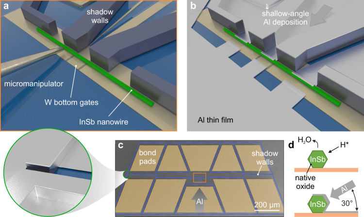
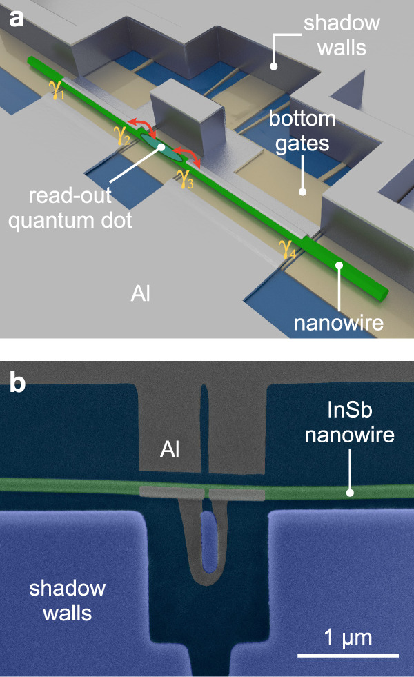
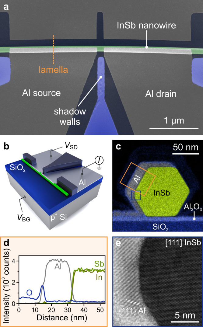
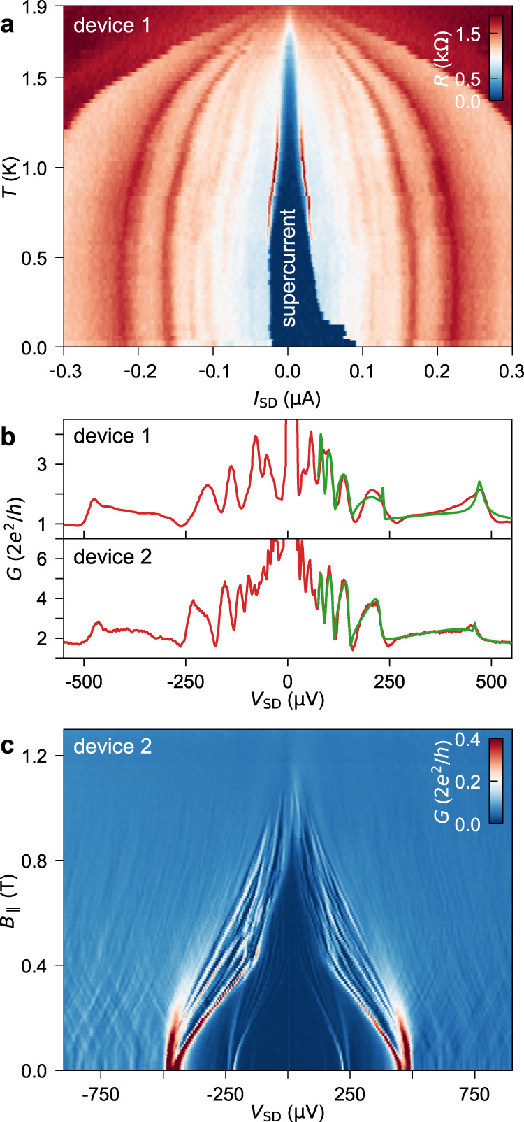
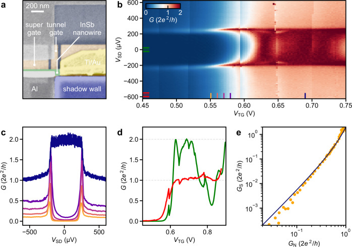
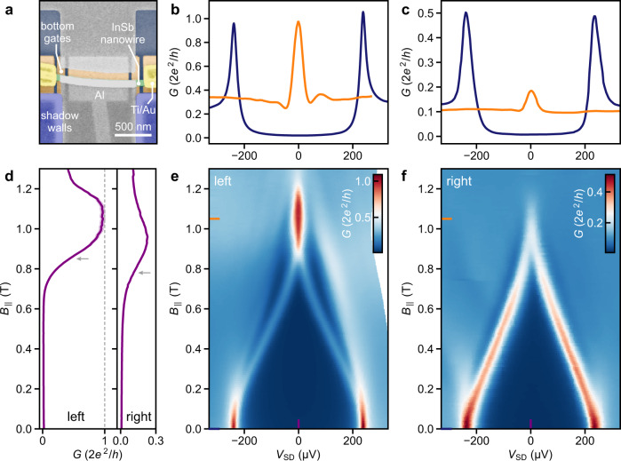
The realization of hybrid superconductor-semiconductor quantum devices, in particular a topological qubit, calls for advanced techniques to readily and reproducibly engineer induced superconductivity in semiconductor nanowires. Here, we introduce an on-chip fabrication paradigm based on shadow walls that offers substantial advances in device quality and reproducibility. It allows for the implementation of hybrid quantum devices and ultimately topological qubits while eliminating fabrication steps such as lithography and etching. This is critical to preserve the integrity and homogeneity of the fragile hybrid interfaces. The approach simplifies the reproducible fabrication of devices with a hard induced superconducting gap and ballistic normal-/superconductor junctions. Large gate-tunable supercurrents and high-order multiple Andreev reflections manifest the exceptional coherence of the resulting nanowire Josephson junctions. Our approach enables the realization of 3-terminal devices, where zero-bias conductance peaks emerge in a magnetic field concurrently at both boundaries of the one-dimensional hybrids.
混合超导体 - 半导体量子器件,特别是拓扑量子比特的实现,需要先进技术来方便且可重复地在半导体纳米线中设计诱导超导性。在此,我们引入一种基于阴影壁的片上制造范例,该范例在器件质量和可重复性方面取得了重大进展。它允许实现混合量子器件,并最终实现拓扑量子比特,同时消除光刻和蚀刻等制造步骤。这对于保持脆弱混合界面的完整性和均匀性至关重要。该方法简化了具有硬诱导超导能隙和弹道正常/超导结的器件的可重复制造。大的栅极可调超导电流和高阶多次安德烈夫反射表明了所得纳米线约瑟夫森结的卓越相干性。我们的方法能够实现三端器件,其中在一维混合体的两个边界处的磁场中同时出现零偏置电导峰。