Zhou Wen, Zheng Li, Ning Zhijun, Cheng Xinhong, Wang Fang, Xu Kaimin, Xu Rui, Liu Zhongyu, Luo Man, Hu Weida, Guo Huijun, Zhou Wenjia, Yu Yuehui
State Key Laboratory of Functional Materials for Informatics, Shanghai Institute of Microsystem and Information Technology, Chinese Academy of Sciences, Shanghai, 200050, P. R. China.
School of Physical Science and Technology, ShanghaiTech University, Shanghai, 201210, P. R. China.
Nat Commun. 2021 Nov 18;12(1):6696. doi: 10.1038/s41467-021-27050-9.
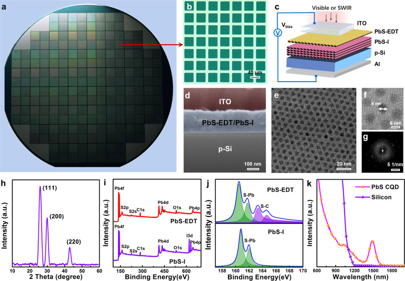
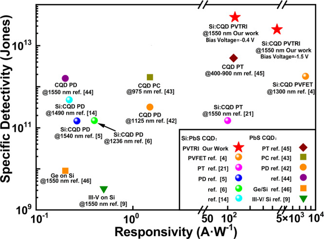
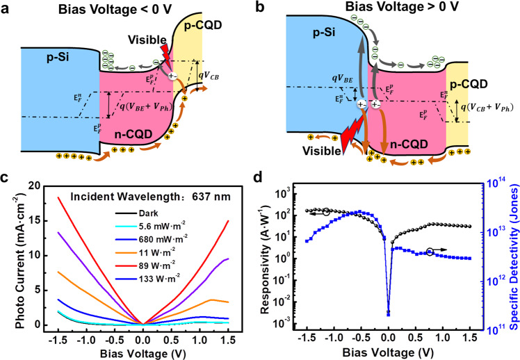
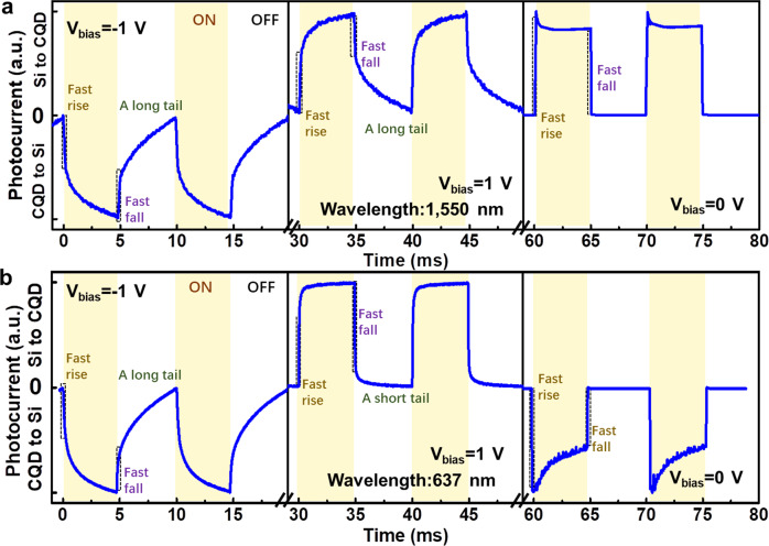
Silicon is widespread in modern electronics, but its electronic bandgap prevents the detection of infrared radiation at wavelengths above 1,100 nanometers, which limits its applications in multiple fields such as night vision, health monitoring and space navigation systems. It is therefore of interest to integrate silicon with infrared-sensitive materials to broaden its detection wavelength. Here we demonstrate a photovoltage triode that can use silicon as the emitter but is also sensitive to infrared spectra owing to the heterointegrated quantum dot light absorber. The photovoltage generated at the quantum dot base region, attracting holes from silicon, leads to high responsivity (exceeding 410 A·W with V of -1.5 V), and a widely self-tunable spectral response. Our device has the maximal specific detectivity (4.73 × 10 Jones with V of -0.4 V) at 1,550 nm among the infrared sensitized silicon detectors, which opens a new path towards infrared and visible imaging in one chip with silicon technology compatibility.
硅在现代电子领域广泛应用,但其电子带隙使得无法检测波长超过1100纳米的红外辐射,这限制了它在夜视、健康监测和太空导航系统等多个领域的应用。因此,将硅与红外敏感材料集成以拓宽其检测波长备受关注。在此,我们展示了一种光电压三极管,它可以将硅用作发射极,但由于异质集成量子点光吸收体,对红外光谱也很敏感。在量子点基区产生的光电压吸引来自硅的空穴,导致高响应度(在-1.5伏偏压下超过410安/瓦)以及广泛的自可调光谱响应。在红外敏化硅探测器中,我们的器件在1550纳米处具有最大比探测率(在-0.4伏偏压下为4.73×10琼斯),这为利用硅技术兼容性在同一芯片上实现红外和可见光成像开辟了一条新途径。