• 文献检索
  • 文档翻译
  • 深度研究
  • 学术资讯
  • Suppr Zotero 插件Zotero 插件
  • 邀请有礼
  • 套餐&价格
  • 历史记录
应用&插件
Suppr Zotero 插件Zotero 插件浏览器插件Mac 客户端Windows 客户端微信小程序
定价
高级版会员购买积分包购买API积分包
服务
文献检索文档翻译深度研究API 文档MCP 服务
关于我们
关于 Suppr公司介绍联系我们用户协议隐私条款
关注我们

Suppr 超能文献

核心技术专利:CN118964589B侵权必究
粤ICP备2023148730 号-1Suppr @ 2026

文献检索

告别复杂PubMed语法,用中文像聊天一样搜索,搜遍4000万医学文献。AI智能推荐,让科研检索更轻松。

立即免费搜索

文件翻译

保留排版,准确专业,支持PDF/Word/PPT等文件格式,支持 12+语言互译。

免费翻译文档

深度研究

AI帮你快速写综述,25分钟生成高质量综述,智能提取关键信息,辅助科研写作。

立即免费体验

沟道厚度对高性能InSnO薄膜晶体管电学性能及稳定性的影响

Effects of Channel Thickness on Electrical Performance and Stability of High-Performance InSnO Thin-Film Transistors.

作者信息

Li Qi, Dong Junchen, Han Dedong, Wang Yi

机构信息

Institute of Microelectronics, Peking University, Beijing 100871, China.

School of Information & Communication Engineering, Beijing Information Science & Technology University, Beijing 100101, China.

出版信息

Membranes (Basel). 2021 Nov 26;11(12):929. doi: 10.3390/membranes11120929.

DOI:10.3390/membranes11120929
PMID:34940430
原文链接:https://pmc.ncbi.nlm.nih.gov/articles/PMC8706019/
Abstract

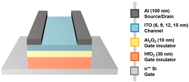
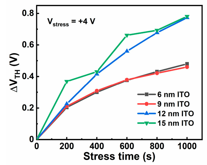
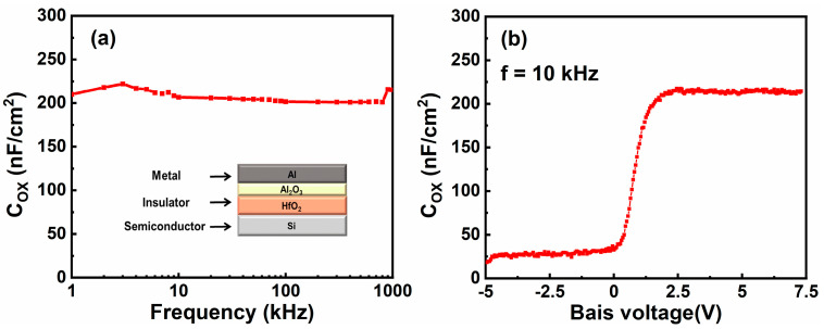
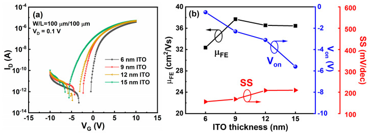
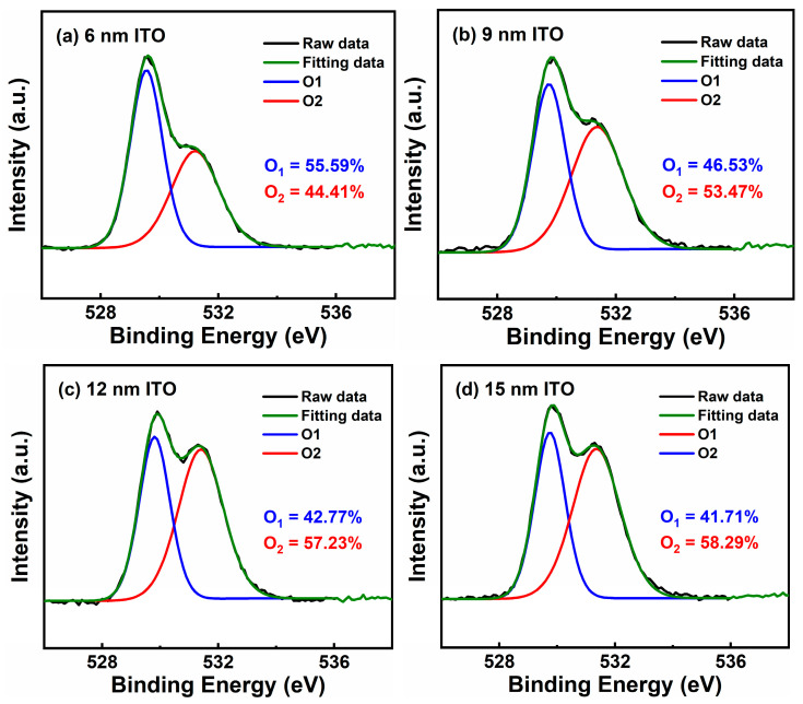
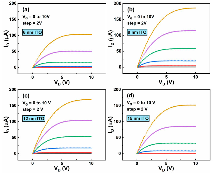
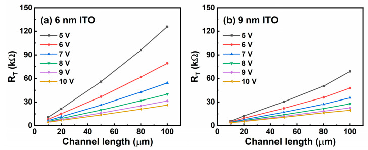
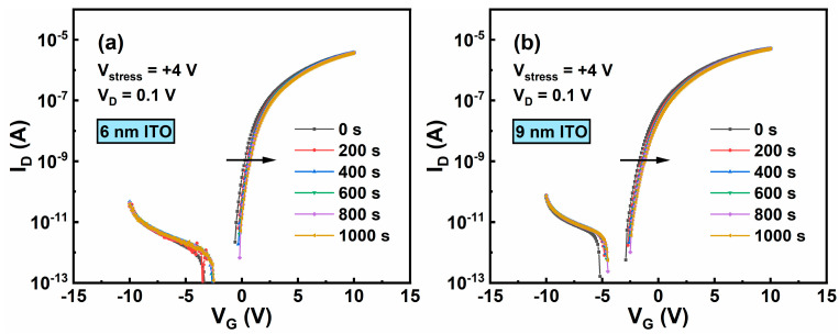
InSnO (ITO) thin-film transistors (TFTs) attract much attention in fields of displays and low-cost integrated circuits (IC). In the present work, we demonstrate the high-performance, robust ITO TFTs that fabricated at process temperature no higher than 100 °C. The influences of channel thickness (t, respectively, 6, 9, 12, and 15 nm) on device performance and positive bias stress (PBS) stability of the ITO TFTs are examined. We found that content of oxygen defects positively correlates with t, leading to increases of both trap states as well as carrier concentration and synthetically determining electrical properties of the ITO TFTs. Interestingly, the ITO TFTs with a t of 9 nm exhibit the best performance and PBS stability, and typical electrical properties include a field-effect mobility (µ) of 37.69 cm/Vs, a V of -2.3 V, a SS of 167.49 mV/decade, and an on-off current ratio over 10. This work paves the way for practical application of the ITO TFTs.

摘要

氧化铟锡(ITO)薄膜晶体管(TFT)在显示器和低成本集成电路(IC)领域备受关注。在本工作中,我们展示了在不高于100°C的工艺温度下制造的高性能、稳健的ITO TFT。研究了沟道厚度(t,分别为6、9、12和15纳米)对ITO TFT器件性能和正偏压应力(PBS)稳定性的影响。我们发现氧缺陷含量与t呈正相关,导致陷阱态以及载流子浓度增加,并综合决定了ITO TFT的电学性能。有趣的是,沟道厚度为9纳米的ITO TFT表现出最佳性能和PBS稳定性,典型电学性能包括场效应迁移率(µ)为37.69厘米²/伏·秒、阈值电压(Vth)为-2.3伏、亚阈值摆幅(SS)为167.49毫伏/十倍频程,以及开/关电流比超过10。这项工作为ITO TFT的实际应用铺平了道路。

https://cdn.ncbi.nlm.nih.gov/pmc/blobs/c078/8706019/7c6241b83121/membranes-11-00929-g010.jpg
https://cdn.ncbi.nlm.nih.gov/pmc/blobs/c078/8706019/78fc3cb731f8/membranes-11-00929-g001.jpg
https://cdn.ncbi.nlm.nih.gov/pmc/blobs/c078/8706019/cc5bfac308c8/membranes-11-00929-g002.jpg
https://cdn.ncbi.nlm.nih.gov/pmc/blobs/c078/8706019/c6c92f8f1aa5/membranes-11-00929-g003.jpg
https://cdn.ncbi.nlm.nih.gov/pmc/blobs/c078/8706019/8a27acb96993/membranes-11-00929-g004.jpg
https://cdn.ncbi.nlm.nih.gov/pmc/blobs/c078/8706019/cb588d57df7f/membranes-11-00929-g005.jpg
https://cdn.ncbi.nlm.nih.gov/pmc/blobs/c078/8706019/9dcdc4bd6931/membranes-11-00929-g006.jpg
https://cdn.ncbi.nlm.nih.gov/pmc/blobs/c078/8706019/207361920aef/membranes-11-00929-g007.jpg
https://cdn.ncbi.nlm.nih.gov/pmc/blobs/c078/8706019/704533608fe4/membranes-11-00929-g008a.jpg
https://cdn.ncbi.nlm.nih.gov/pmc/blobs/c078/8706019/d72cf0d95991/membranes-11-00929-g009a.jpg
https://cdn.ncbi.nlm.nih.gov/pmc/blobs/c078/8706019/7c6241b83121/membranes-11-00929-g010.jpg

相似文献

1
Effects of Channel Thickness on Electrical Performance and Stability of High-Performance InSnO Thin-Film Transistors.沟道厚度对高性能InSnO薄膜晶体管电学性能及稳定性的影响
Membranes (Basel). 2021 Nov 26;11(12):929. doi: 10.3390/membranes11120929.
2
Effects of Source/Drain Electrodes on the Performance of InSnO Thin-Film Transistors.源极/漏极电极对InSnO薄膜晶体管性能的影响。
Micromachines (Basel). 2022 Nov 2;13(11):1896. doi: 10.3390/mi13111896.
3
Structural Engineering Effects on Hump Characteristics of ZnO/InSnO Heterojunction Thin-Film Transistors.结构工程对ZnO/InSnO异质结薄膜晶体管驼峰特性的影响
Nanomaterials (Basel). 2022 Mar 31;12(7):1167. doi: 10.3390/nano12071167.
4
Enhancing the Carrier Mobility and Bias Stability in Metal-Oxide Thin Film Transistors with Bilayer InSnO/a-InGaZnO Heterojunction Structure.通过双层InSnO/a-InGaZnO异质结结构提高金属氧化物薄膜晶体管中的载流子迁移率和偏置稳定性。
Micromachines (Basel). 2024 Apr 11;15(4):512. doi: 10.3390/mi15040512.
5
Improving Performance of Tin-Doped-Zinc-Oxide Thin-Film Transistors by Optimizing Channel Structure.通过优化沟道结构提高掺锡氧化锌薄膜晶体管的性能
Sci Rep. 2019 Nov 20;9(1):17175. doi: 10.1038/s41598-019-53766-2.
6
One-Step Synergistic Treatment Approach for High Performance Amorphous InGaZnO Thin-Film Transistors Fabricated at Room Temperature.室温制备高性能非晶铟镓锌氧化物薄膜晶体管的一步协同处理方法。
Nanomaterials (Basel). 2022 Oct 5;12(19):3481. doi: 10.3390/nano12193481.
7
Low-voltage operation of ZrO2-gated n-type thin-film transistors based on a channel formed by hybrid phases of SnO and SnO2.基于由SnO和SnO2混合相形成的沟道的ZrO2栅控n型薄膜晶体管的低压操作。
ACS Appl Mater Interfaces. 2015 Jul 22;7(28):15129-37. doi: 10.1021/acsami.5b02941. Epub 2015 Jul 13.
8
Improvement of Electrical Characteristics and Stability of Amorphous Indium Gallium Zinc Oxide Thin Film Transistors Using Nitrocellulose Passivation Layer.使用硝化纤维素钝化层改善非晶态铟镓锌氧化物薄膜晶体管的电学特性和稳定性。
ACS Appl Mater Interfaces. 2017 Apr 19;9(15):13278-13285. doi: 10.1021/acsami.7b00257. Epub 2017 Apr 4.
9
Fully transparent high performance thin film transistors with bilayer ITO/Al-Sn-Zn-O channel structures fabricated on glass substrate.在玻璃衬底上制备具有双层 ITO/Al-Sn-Zn-O 沟道结构的完全透明高性能薄膜晶体管。
Sci Rep. 2017 May 4;7(1):1497. doi: 10.1038/s41598-017-01691-7.
10
An All Oxide-Based Imperceptible Thin-Film Transistor with Humidity Sensing Properties.一种具有湿度传感特性的全氧化物基隐形薄膜晶体管。
Materials (Basel). 2017 May 13;10(5):530. doi: 10.3390/ma10050530.

引用本文的文献

1
Control of electrical properties in solution-processed ATO thin-film transistors through gallium doping.通过镓掺杂控制溶液法制备的氧化铟锡薄膜晶体管的电学性能。
RSC Adv. 2025 Apr 28;15(17):13595-13602. doi: 10.1039/d5ra00207a. eCollection 2025 Apr 22.
2
Enhancing the Stability and Mobility of TFTs via Indium-Tungsten Oxide and Zinc Oxide Engineered Heterojunction Channels Annealed in Oxygen Ambient.通过在氧气环境中退火的铟钨氧化物和氧化锌工程异质结通道增强薄膜晶体管的稳定性和迁移率。
Nanomaterials (Basel). 2024 Jul 26;14(15):1252. doi: 10.3390/nano14151252.
3
Effects of Source/Drain Electrodes on the Performance of InSnO Thin-Film Transistors.

本文引用的文献

1
Fully Printed High-Performance n-Type Metal Oxide Thin-Film Transistors Utilizing Coffee-Ring Effect.利用咖啡环效应的全印刷高性能n型金属氧化物薄膜晶体管
Nanomicro Lett. 2021 Aug 3;13(1):164. doi: 10.1007/s40820-021-00694-4.
2
Wide Bandgap Oxide Semiconductors: from Materials Physics to Optoelectronic Devices.宽带隙氧化物半导体:从材料物理到光电器件
Adv Mater. 2021 Dec;33(50):e2006230. doi: 10.1002/adma.202006230. Epub 2021 Apr 1.
3
Nanometre-thin indium tin oxide for advanced high-performance electronics.用于先进高性能电子设备的纳米级超薄氧化铟锡
源极/漏极电极对InSnO薄膜晶体管性能的影响。
Micromachines (Basel). 2022 Nov 2;13(11):1896. doi: 10.3390/mi13111896.
4
Thin-Film Transistors.薄膜晶体管
Membranes (Basel). 2022 Apr 9;12(4):411. doi: 10.3390/membranes12040411.
5
Structural Engineering Effects on Hump Characteristics of ZnO/InSnO Heterojunction Thin-Film Transistors.结构工程对ZnO/InSnO异质结薄膜晶体管驼峰特性的影响
Nanomaterials (Basel). 2022 Mar 31;12(7):1167. doi: 10.3390/nano12071167.
Nat Mater. 2019 Oct;18(10):1091-1097. doi: 10.1038/s41563-019-0455-8. Epub 2019 Aug 12.
4
Efficient Suppression of Defects and Charge Trapping in High Density In-Sn-Zn-O Thin Film Transistor Prepared using Microwave-Assisted Sputter.采用微波辅助溅射法制备的高密度 In-Sn-Zn-O 薄膜晶体管中缺陷和电荷俘获的有效抑制。
ACS Appl Mater Interfaces. 2017 Oct 25;9(42):36962-36970. doi: 10.1021/acsami.7b08065. Epub 2017 Oct 16.
5
Enhanced Performance in Al-Doped ZnO Based Transparent Flexible Transparent Thin-Film Transistors Due to Oxygen Vacancy in ZnO Film with Zn-Al-O Interfaces Fabricated by Atomic Layer Deposition.原子层沉积法制备的 Zn-Al-O 界面 ZnO 薄膜中氧空位对掺铝氧化锌基透明柔性透明薄膜晶体管性能的增强作用。
ACS Appl Mater Interfaces. 2017 Apr 5;9(13):11711-11720. doi: 10.1021/acsami.7b02609. Epub 2017 Mar 27.
6
Oxide semiconductor thin-film transistors: a review of recent advances.氧化物半导体薄膜晶体管:研究进展综述。
Adv Mater. 2012 Jun 12;24(22):2945-86. doi: 10.1002/adma.201103228. Epub 2012 May 10.