D'Auria Vincenzo, Bruzzone Pierluigi, Meyer Mickael Sebastian, Castro Enrique Rodriguez, Sgobba Stefano
Ecole Polytechnique Fédérale de Lausanne (EPFL), Swiss Plasma Center (SPC), The Paul Scherrer Institute (PSI), CH-5232 Villigen, Switzerland.
European Council for Nuclear Research (CERN), CH-1211 Geneva, Switzerland.
Materials (Basel). 2021 Dec 24;15(1):125. doi: 10.3390/ma15010125.
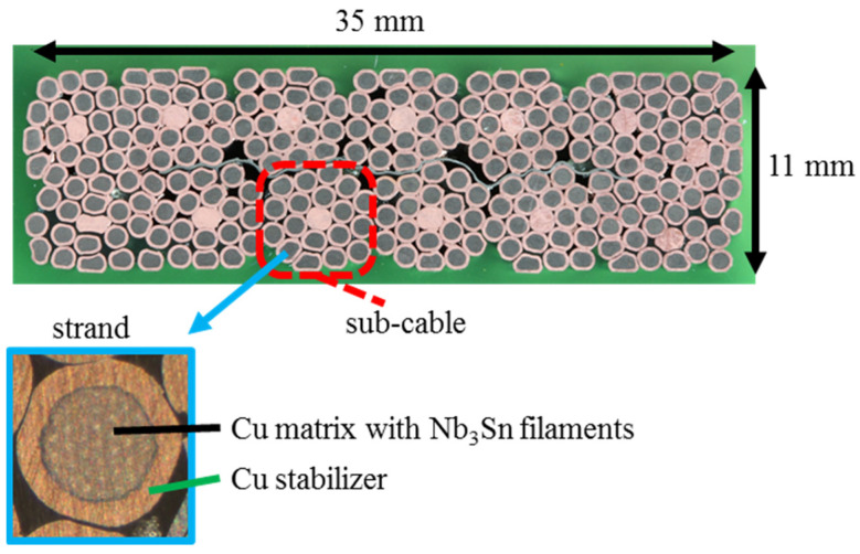
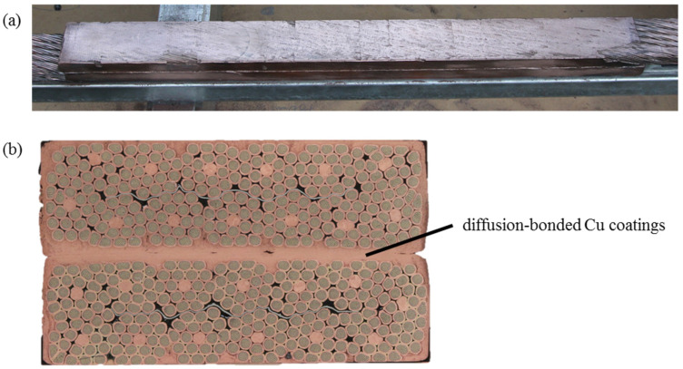
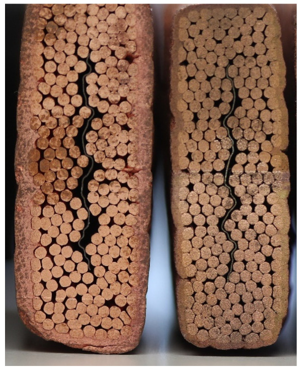
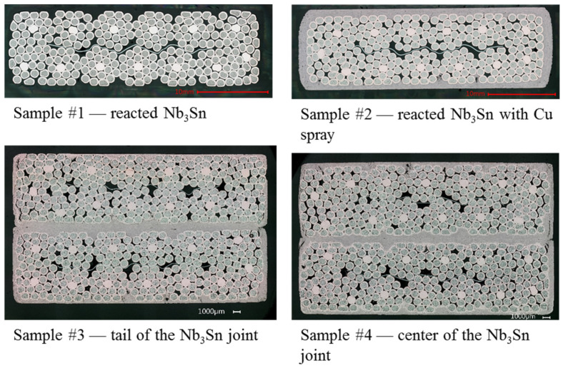
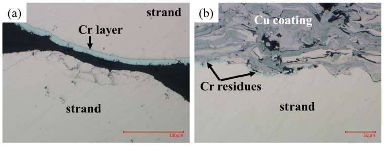
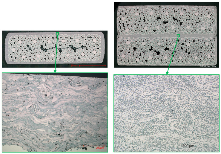
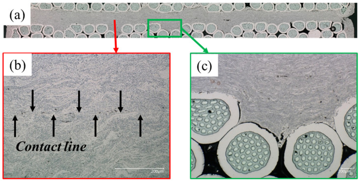
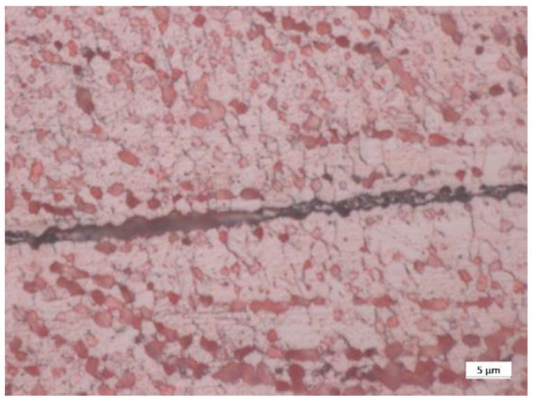
This manuscript reports on the application of copper thermal spraying in the manufacturing process of an electrical connection between NbSn cables for superconducting magnets of fusion reactors. The joint is realized through diffusion bonding of the sprayed coating of the two cables. The main requirement for such a connection is its electrical resistance, which must be below 1 nΩ at B = 8 T, I = 63.3 kA and T = 4.5 K. Micrographs of the joint prototype were taken to relate the joint resistance with its microstructure and to provide feedback on the manufacturing process. Optical microscopy (OM) was used to evaluate the grain size of the coating, presence of oxide phases and to analyze the jointed surfaces. Scanning electron microscopy (SEM) and, in particular, energy-dispersive X-ray spectroscopy (EDX) were used to confirm the elemental composition of specimens extracted from the prototype. It is shown that the copper coating has an oxide concentration of 40%. Despite this, the resistance of the prototype is 0.48 nΩ in operating conditions, as the oxides are in globular form. The contact ratio between the jointed surfaces is about 95%. In addition, residual resistivity ratio (RRR) measurements were carried out to quantify the electrical quality of the Cu coating.
本手稿报道了铜热喷涂在聚变反应堆超导磁体铌锡电缆电气连接制造过程中的应用。该接头通过两根电缆喷涂涂层的扩散结合实现。这种连接的主要要求是其电阻,在B = 8 T、I = 63.3 kA和T = 4.5 K时必须低于1 nΩ。拍摄接头原型的显微照片,以关联接头电阻与其微观结构,并为制造过程提供反馈。光学显微镜(OM)用于评估涂层的晶粒尺寸、氧化物相的存在情况以及分析连接表面。扫描电子显微镜(SEM),特别是能量色散X射线光谱(EDX)用于确认从原型中提取的试样的元素组成。结果表明,铜涂层的氧化物浓度为40%。尽管如此,由于氧化物呈球状,原型在运行条件下的电阻为0.48 nΩ。连接表面之间的接触率约为95%。此外,还进行了剩余电阻率比(RRR)测量,以量化铜涂层的电气质量。