Rejhon Martin, Dedic Vaclav, Grill Roman, Franc Jan, Roy Utpal N, James Ralph B
Faculty of Mathematics and Physics, Charles University, Ke Karlovu 3, 12116 Prague, Czech Republic.
Tandon School of Engineering, New York University, Brooklyn, NY 11201, USA.
Sensors (Basel). 2021 Dec 28;22(1):171. doi: 10.3390/s22010171.
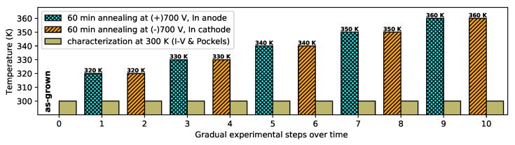
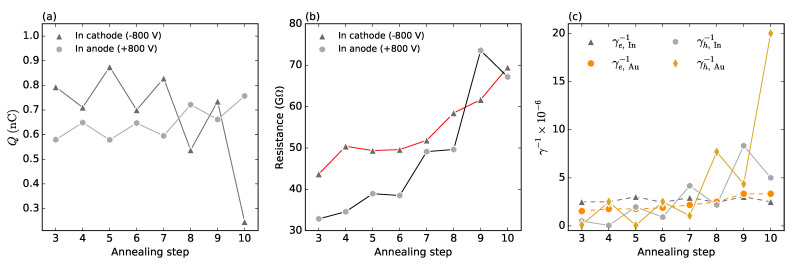
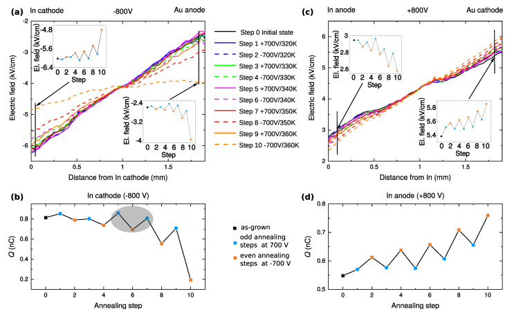
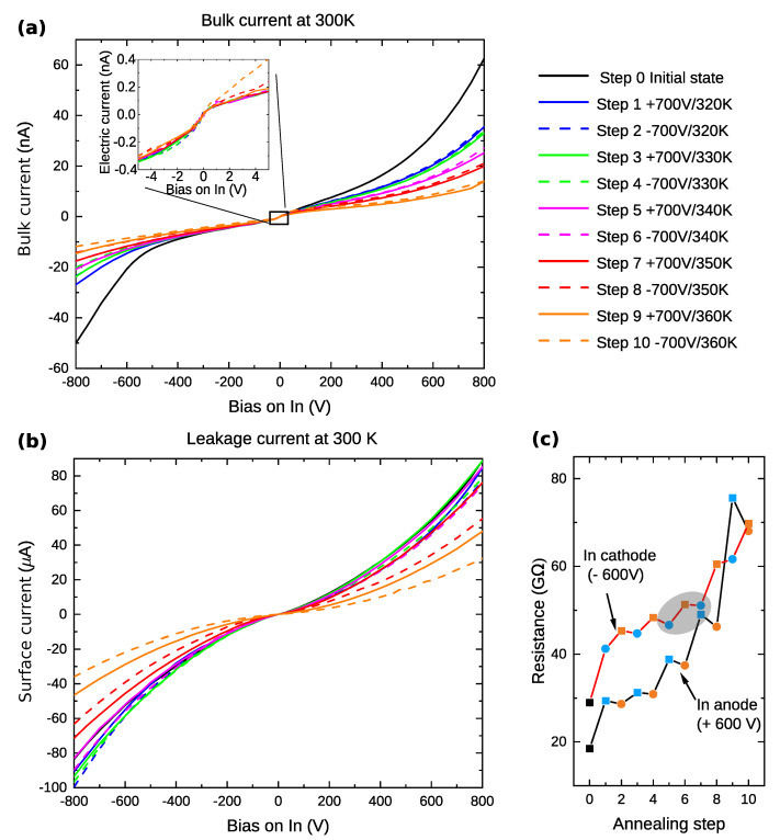
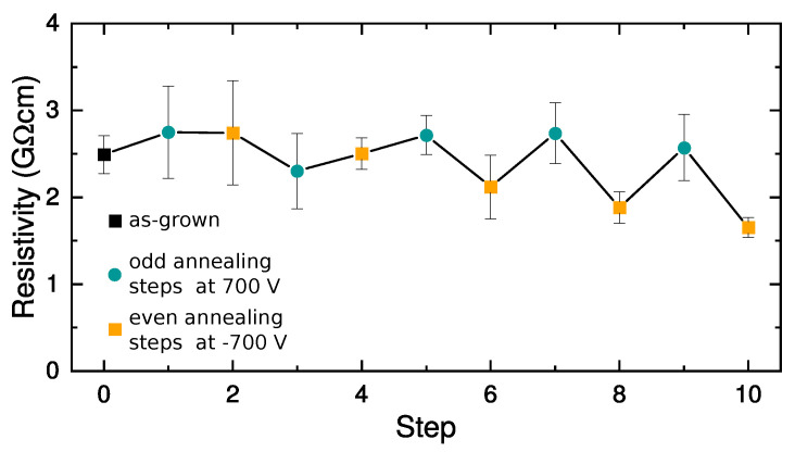
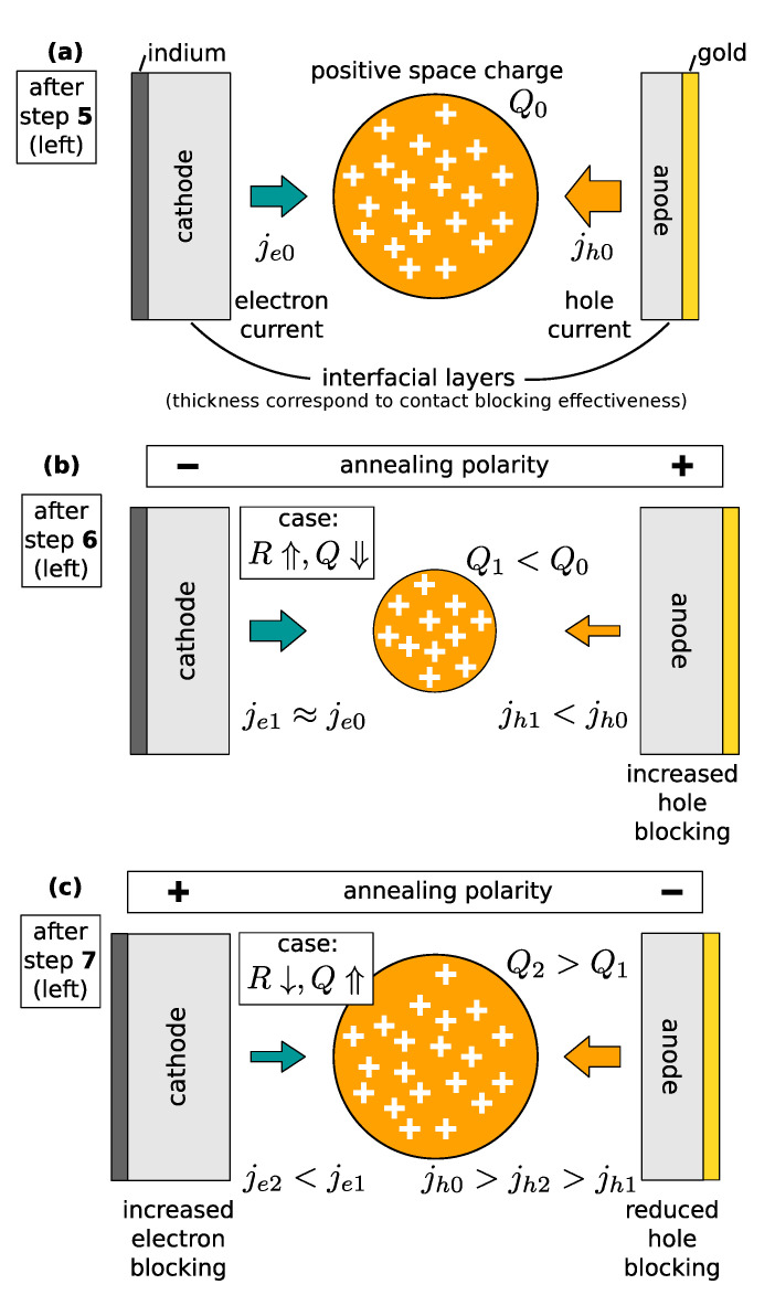
We performed a gradual low-temperature annealing up to 360 K on a CdZnTeSe radiation detector equipped with gold and indium electrodes under bias at both polarities. We observed significant changes in the detector's resistance and space-charge accumulation. This could potentially lead to the control and improvement of the electronic properties of the detector because the changes are accompanied with the reduction in the bulk dark current and surface leakage current. In this article, we present the results of a detailed study of the internal electric field and conductivity changes in CdZnTeSe detector for various annealing steps under bias taking into account different polarities during annealing and subsequent characterization. We observed that low-temperature annealing results in an increase in the barrier height at the contacts that, in general, reduces the dark current and decreases the positive space charge present in the sample compared to the pre-annealed condition.
我们在一个配备金和铟电极的CdZnTeSe辐射探测器上,在两种极性的偏压下进行了逐步升温至360K的低温退火。我们观察到探测器电阻和空间电荷积累有显著变化。这可能潜在地导致探测器电子性能的控制和改善,因为这些变化伴随着体暗电流和表面漏电流的降低。在本文中,我们展示了在考虑退火过程中的不同极性以及后续表征的情况下,对处于偏压下的CdZnTeSe探测器在不同退火步骤下内部电场和电导率变化的详细研究结果。我们观察到低温退火导致接触处势垒高度增加,总体而言,与退火前的状态相比,这降低了暗电流并减少了样品中存在的正空间电荷。