Department of Computer Science and Communications Technologies, Vilnius Gediminas Technical University, 03227 Vilnius, Lithuania.
Sensors (Basel). 2022 Jan 26;22(3):964. doi: 10.3390/s22030964.
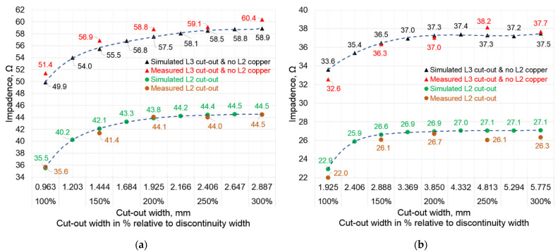
The modern era of technology contains a myriad of high-speed standards and proprietary serial digital protocols, which evolve alongside the microwave and RF realm. The increasing data rate push the requirements for hardware design, including modern printed circuit boards (PCB). One of these requirements for modern high-speed PCB interfaces are a homogenous track impedance all the way from the source to the load. Even though some high-speed interfaces don't require any external components embedded into the interconnects, there are others which require either passive or active components-or both. Usually, component package land-pads are of fixed size, thus, if not addressed, they create discontinuities and degrade the transmitted signal. To solve this problem, impedance compensation techniques such as reference plane cut-out are employed for multiple case studies covering this topic. This paper presents an original method of finding the optimal cut-out size for the maximum characteristic impedance compensation in high-density multilayer PCB designs, which has been verified via theoretical estimation, computer simulation, and practical measurement results. Track-to-discontinuity ratios of 1:1.75, 1:2.5, and 1:5.0 were selected in order to resemble most practical design scenarios on a 6-layer standard thickness PCB. The measurements and simulations revealed that the compensated impedance saturation occurs at (150-250%) cut-out widths for a 50 Ω microstrip.
现代科技时代包含了众多高速标准和专有串行数字协议,这些协议与微波和射频领域一起发展。数据传输速率的提高推动了硬件设计的要求,包括现代印刷电路板(PCB)。现代高速 PCB 接口的要求之一是从源到负载的均匀轨迹阻抗。尽管有些高速接口不需要在互连中嵌入任何外部组件,但有些接口需要无源或有源组件,或者两者都需要。通常,组件封装焊盘的尺寸是固定的,因此,如果不加以解决,它们会产生不连续性并劣化传输信号。为了解决这个问题,采用了阻抗补偿技术,例如参考平面切孔,对涵盖这一主题的多个案例进行了研究。本文提出了一种在高密度多层 PCB 设计中找到最佳切孔尺寸以实现最大特征阻抗补偿的原始方法,该方法已通过理论估算、计算机模拟和实际测量结果进行了验证。选择了 1:1.75、1:2.5 和 1:5.0 的走线到不连续性比,以模拟 6 层标准厚度 PCB 上的大多数实际设计情况。测量和模拟结果表明,对于 50 Ω 微带线,补偿阻抗饱和发生在(150-250%)切孔宽度处。