• 文献检索
  • 文档翻译
  • 深度研究
  • 学术资讯
  • Suppr Zotero 插件Zotero 插件
  • 邀请有礼
  • 套餐&价格
  • 历史记录
应用&插件
Suppr Zotero 插件Zotero 插件浏览器插件Mac 客户端Windows 客户端微信小程序
定价
高级版会员购买积分包购买API积分包
服务
文献检索文档翻译深度研究API 文档MCP 服务
关于我们
关于 Suppr公司介绍联系我们用户协议隐私条款
关注我们

Suppr 超能文献

核心技术专利:CN118964589B侵权必究
粤ICP备2023148730 号-1Suppr @ 2026

文献检索

告别复杂PubMed语法,用中文像聊天一样搜索,搜遍4000万医学文献。AI智能推荐,让科研检索更轻松。

立即免费搜索

文件翻译

保留排版,准确专业,支持PDF/Word/PPT等文件格式,支持 12+语言互译。

免费翻译文档

深度研究

AI帮你快速写综述,25分钟生成高质量综述,智能提取关键信息,辅助科研写作。

立即免费体验

基于范德华界面晶体管的具有偏置可调谐光谱的光源。

Light sources with bias tunable spectrum based on van der Waals interface transistors.

作者信息

Henck Hugo, Mauro Diego, Domaretskiy Daniil, Philippi Marc, Memaran Shahriar, Zheng Wenkai, Lu Zhengguang, Shcherbakov Dmitry, Lau Chun Ning, Smirnov Dmitry, Balicas Luis, Watanabe Kenji, Taniguchi Takashi, Fal'ko Vladimir I, Gutiérrez-Lezama Ignacio, Ubrig Nicolas, Morpurgo Alberto F

机构信息

Department of Quantum Matter Physics, University of Geneva, 24 Quai Ernest Ansermet, 1211, Geneva, Switzerland.

Department of Applied Physics, University of Geneva, 24 Quai Ernest Ansermet, 1211, Geneva, Switzerland.

出版信息

Nat Commun. 2022 Jul 7;13(1):3917. doi: 10.1038/s41467-022-31605-9.

DOI:10.1038/s41467-022-31605-9
PMID:35798736
原文链接:https://pmc.ncbi.nlm.nih.gov/articles/PMC9263129/
Abstract

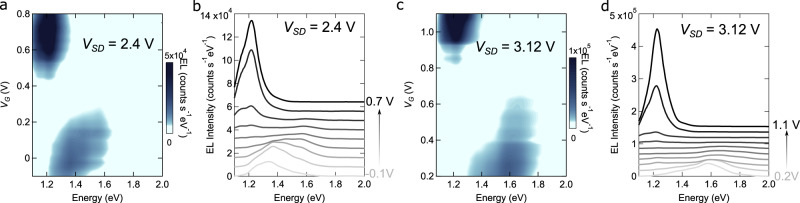
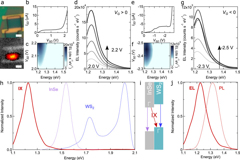
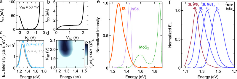
Light-emitting electronic devices are ubiquitous in key areas of current technology, such as data communications, solid-state lighting, displays, and optical interconnects. Controlling the spectrum of the emitted light electrically, by simply acting on the device bias conditions, is an important goal with potential technological repercussions. However, identifying a material platform enabling broad electrical tuning of the spectrum of electroluminescent devices remains challenging. Here, we propose light-emitting field-effect transistors based on van der Waals interfaces of atomically thin semiconductors as a promising class of devices to achieve this goal. We demonstrate that large spectral changes in room-temperature electroluminescence can be controlled both at the device assembly stage -by suitably selecting the material forming the interfaces- and on-chip, by changing the bias to modify the device operation point. Even though the precise relation between device bias and kinetics of the radiative transitions remains to be understood, our experiments show that the physical mechanism responsible for light emission is robust, making these devices compatible with simple large areas device production methods.

摘要

发光电子器件在当前技术的关键领域无处不在,如数据通信、固态照明、显示器和光互连。通过简单地改变器件偏置条件来电控制发射光的光谱,是一个具有潜在技术影响的重要目标。然而,找到一个能实现电致发光器件光谱广泛电调谐的材料平台仍然具有挑战性。在此,我们提出基于原子级薄半导体范德华界面的发光场效应晶体管,作为实现这一目标的一类有前景的器件。我们证明,室温电致发光中的大幅光谱变化既可以在器件组装阶段通过适当选择形成界面的材料来控制,也可以在芯片上通过改变偏置来修改器件工作点进行控制。尽管器件偏置与辐射跃迁动力学之间的确切关系仍有待了解,但我们的实验表明,负责发光的物理机制是稳健的,这使得这些器件能够与简单的大面积器件制造方法兼容。

https://cdn.ncbi.nlm.nih.gov/pmc/blobs/ec8f/9263129/ecc250e23fcf/41467_2022_31605_Fig6_HTML.jpg
https://cdn.ncbi.nlm.nih.gov/pmc/blobs/ec8f/9263129/a8ffd17ed36b/41467_2022_31605_Fig1_HTML.jpg
https://cdn.ncbi.nlm.nih.gov/pmc/blobs/ec8f/9263129/181330a62f78/41467_2022_31605_Fig2_HTML.jpg
https://cdn.ncbi.nlm.nih.gov/pmc/blobs/ec8f/9263129/5263ca6316eb/41467_2022_31605_Fig3_HTML.jpg
https://cdn.ncbi.nlm.nih.gov/pmc/blobs/ec8f/9263129/44ea54820991/41467_2022_31605_Fig4_HTML.jpg
https://cdn.ncbi.nlm.nih.gov/pmc/blobs/ec8f/9263129/aa6d511c26f3/41467_2022_31605_Fig5_HTML.jpg
https://cdn.ncbi.nlm.nih.gov/pmc/blobs/ec8f/9263129/ecc250e23fcf/41467_2022_31605_Fig6_HTML.jpg

相似文献

1
Light sources with bias tunable spectrum based on van der Waals interface transistors.基于范德华界面晶体管的具有偏置可调谐光谱的光源。
Nat Commun. 2022 Jul 7;13(1):3917. doi: 10.1038/s41467-022-31605-9.
2
Room-temperature electrical control of polarization and emission angle in a cavity-integrated 2D pulsed LED.腔集成二维脉冲发光二极管中极化和发射角的室温电控制
Nat Commun. 2022 Aug 19;13(1):4884. doi: 10.1038/s41467-022-32292-2.
3
Electroluminescent Devices Based on 2D Semiconducting Transition Metal Dichalcogenides.基于二维半导体过渡金属二卤化物的电致发光器件。
Adv Mater. 2018 Nov;30(47):e1802687. doi: 10.1002/adma.201802687. Epub 2018 Aug 17.
4
Design of van der Waals interfaces for broad-spectrum optoelectronics.用于广谱光电子学的范德华界面设计
Nat Mater. 2020 Mar;19(3):299-304. doi: 10.1038/s41563-019-0601-3. Epub 2020 Feb 3.
5
Single Defect Light-Emitting Diode in a van der Waals Heterostructure.单层范德华异质结构中的单缺陷发光二极管。
Nano Lett. 2016 Jun 8;16(6):3944-8. doi: 10.1021/acs.nanolett.6b01580. Epub 2016 May 26.
6
Multioperation-Mode Light-Emitting Field-Effect Transistors Based on van der Waals Heterostructure.基于范德华异质结构的多操作模式发光场效应晶体管
Adv Mater. 2020 Oct;32(43):e2003567. doi: 10.1002/adma.202003567. Epub 2020 Sep 11.
7
Black phosphorus-based van der Waals heterostructures for mid-infrared light-emission applications.用于中红外发光应用的基于黑磷的范德华异质结构。
Light Sci Appl. 2020 Jul 2;9:114. doi: 10.1038/s41377-020-00356-x. eCollection 2020.
8
Van der Waals contacts between three-dimensional metals and two-dimensional semiconductors.三维金属与二维半导体之间的范德华接触。
Nature. 2019 Apr;568(7750):70-74. doi: 10.1038/s41586-019-1052-3. Epub 2019 Mar 27.
9
Nanocavity Integrated van der Waals Heterostructure Light-Emitting Tunneling Diode.纳米腔集成范德瓦尔斯异质结构发光隧道二极管。
Nano Lett. 2017 Jan 11;17(1):200-205. doi: 10.1021/acs.nanolett.6b03801. Epub 2016 Dec 12.
10
Two-dimensional transition metal dichalcogenides as atomically thin semiconductors: opportunities and challenges.二维过渡金属二卤族化合物作为原子层状半导体:机遇与挑战。
Chem Soc Rev. 2015 Dec 21;44(24):8859-76. doi: 10.1039/c5cs00507h. Epub 2015 Oct 19.

引用本文的文献

1
Emergent 2D van der Waals materials photonic sources.二维范德华材料的紧急光子源。
Nanophotonics. 2025 Mar 11;14(10):1475-1507. doi: 10.1515/nanoph-2024-0702. eCollection 2025 May.
2
Giant Light Emission Enhancement in Strain-Engineered InSe/MS (M = Mo or W) van der Waals Heterostructures.应变工程InSe/MS(M = Mo或W)范德华异质结构中的巨光发射增强
Nano Lett. 2025 Mar 5;25(9):3375-3382. doi: 10.1021/acs.nanolett.4c04252. Epub 2025 Feb 5.

本文引用的文献

1
Actively variable-spectrum optoelectronics with black phosphorus.具有黑磷的主动可变光谱光电。
Nature. 2021 Aug;596(7871):232-237. doi: 10.1038/s41586-021-03701-1. Epub 2021 Aug 11.
2
Organic Light-Emitting Transistors Entering a New Development Stage.有机发光晶体管进入新的发展阶段。
Adv Mater. 2021 Aug;33(31):e2007149. doi: 10.1002/adma.202007149. Epub 2021 May 22.
3
Understanding ambipolar transport in MoS field effect transistors: the substrate is the key.理解二硫化钼场效应晶体管中的双极传输:衬底是关键。
Nanotechnology. 2021 Jan 7;32(13):135202. doi: 10.1088/1361-6528/abd27a.
4
Design of van der Waals interfaces for broad-spectrum optoelectronics.用于广谱光电子学的范德华界面设计
Nat Mater. 2020 Mar;19(3):299-304. doi: 10.1038/s41563-019-0601-3. Epub 2020 Feb 3.
5
Electrical control of interlayer exciton dynamics in atomically thin heterostructures.原子层状异质结构中层间激子动力学的电控。
Science. 2019 Nov 15;366(6467):870-875. doi: 10.1126/science.aaw4194.
6
Effective Hexagonal Boron Nitride Passivation of Few-Layered InSe and GaSe to Enhance Their Electronic and Optical Properties.有效六方氮化硼钝化少层 InSe 和 GaSe 以增强其电子和光学性质。
ACS Appl Mater Interfaces. 2019 Nov 20;11(46):43480-43487. doi: 10.1021/acsami.9b13442. Epub 2019 Nov 7.
7
Out-of-plane orientation of luminescent excitons in two-dimensional indium selenide.二维硒化铟中发光激子的面外取向
Nat Commun. 2019 Sep 2;10(1):3913. doi: 10.1038/s41467-019-11920-4.
8
InSe as a case between 3D and 2D layered crystals for excitons.作为一种介于三维和二维层状晶体之间的用于激子的铟硒化物。
Nat Commun. 2019 Aug 2;10(1):3479. doi: 10.1038/s41467-019-11487-0.
9
Upconverted electroluminescence via Auger scattering of interlayer excitons in van der Waals heterostructures.通过范德华异质结构中层间激子的俄歇散射实现的上转换电致发光。
Nat Commun. 2019 May 27;10(1):2335. doi: 10.1038/s41467-019-10323-9.
10
Electroluminescence from multi-particle exciton complexes in transition metal dichalcogenide semiconductors.过渡金属二硫族化合物半导体中多粒子激子复合体的电致发光。
Nat Commun. 2019 Apr 12;10(1):1709. doi: 10.1038/s41467-019-09781-y.