Yang Liang, Wang Zhenhua, Li Mingze, Gao Xuan P A, Zhang Zhidong
Shenyang National Laboratory for Materials Science, Institute of Metal Research, University of Chinese Academy of Sciences, Chinese Academy of Sciences 72 Wenhua Road Shenyang 110016 People's Republic of China.
School of Materials Science and Engineering, University of Science and Technology of China Hefei 230026 China.
Nanoscale Adv. 2019 Apr 17;1(6):2303-2310. doi: 10.1039/c9na00036d. eCollection 2019 Jun 11.
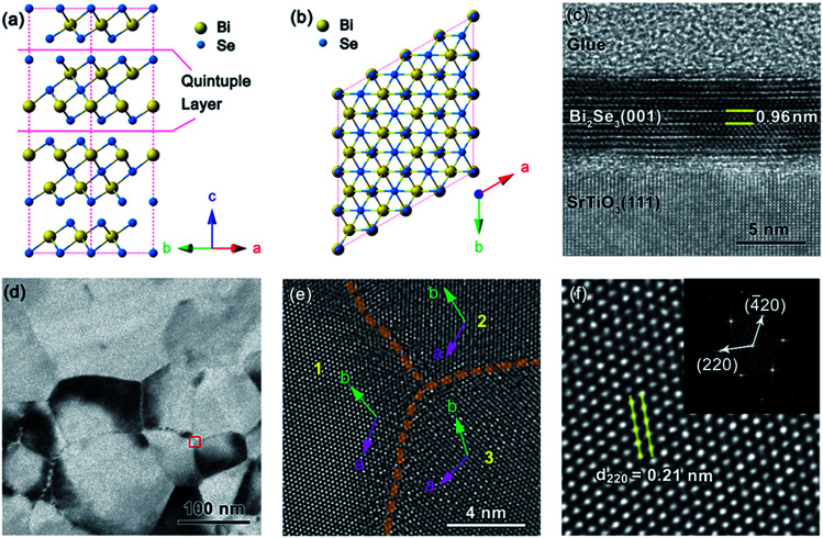
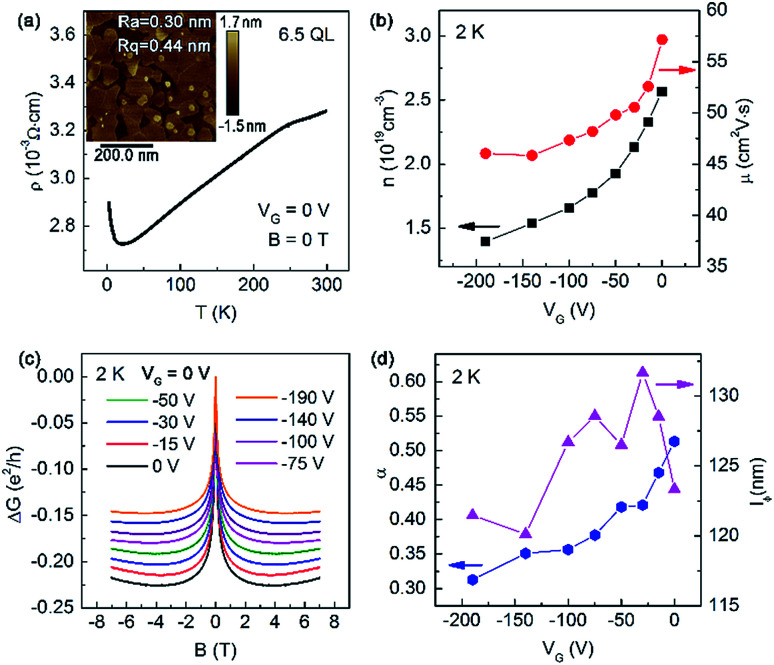
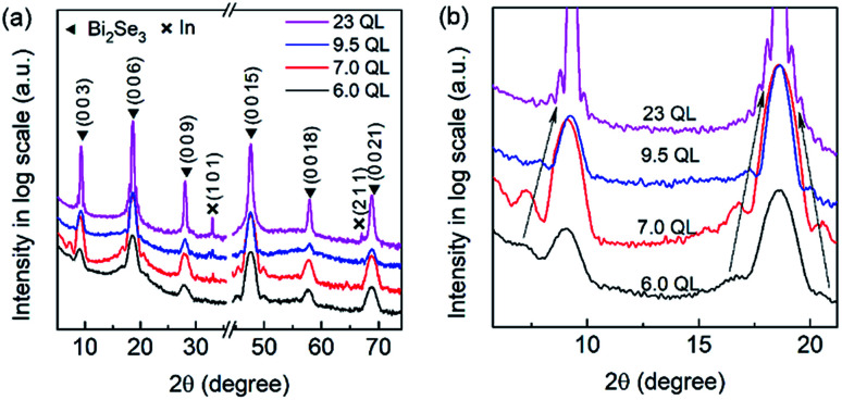
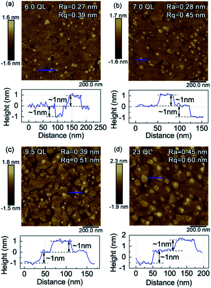
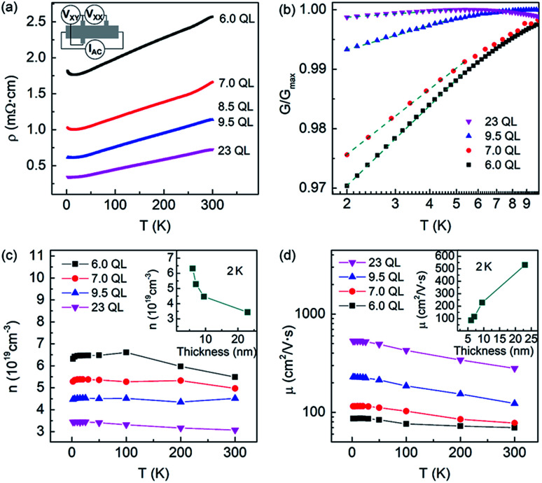
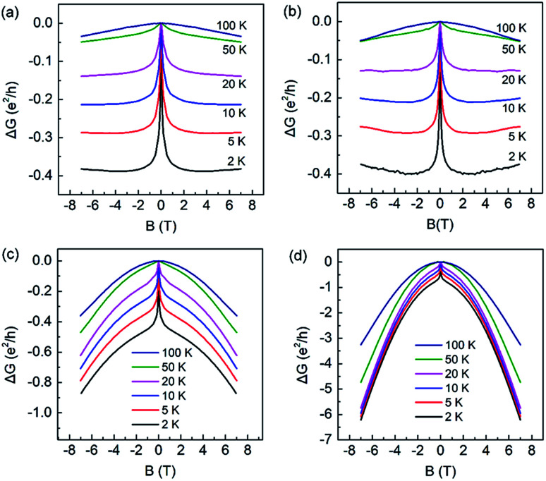
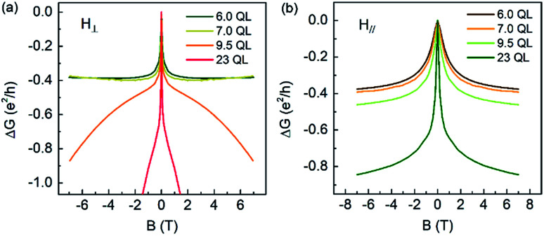
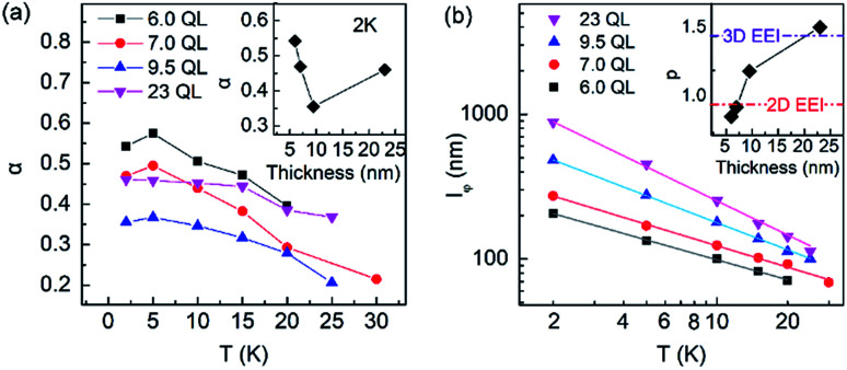
Topological insulator bismuth selenide (BiSe) thin films with a thickness of 6.0 quintuple layers (QL) to 23 QL are deposited using pulsed laser deposition (PLD). The arithmetical mean deviation of the roughness ( ) of these films is less than 0.5 nm, and the root square mean deviation of the roughness ( ) of these films is less than 0.6 nm. Two-dimensional localization and weak antilocalization are observed in the BiSe thin films approaching 6.0 nm, and the origin of weak localization should be a 2D electron gas resulting from the split bulk state. Localization introduced by electron-electron interaction (EEI) is revealed by the temperature dependence of the conductivity. The enhanced contribution of three-dimensional EEI and electron-phonon interaction in the electron dephasing process is found by increasing the thickness. Considering the advantage of stoichiometric transfer in PLD, it is believed that the high quality BiSe thin films might provide more paths for doping and multilayered devices.
采用脉冲激光沉积(PLD)法制备了厚度为6.0个五重层(QL)至23 QL的拓扑绝缘体硒化铋(BiSe)薄膜。这些薄膜的粗糙度算术平均偏差( )小于0.5 nm,粗糙度均方根偏差( )小于0.6 nm。在接近6.0 nm的BiSe薄膜中观察到二维局域化和弱反局域化现象,弱局域化的起源应为分裂体态产生的二维电子气。电导率的温度依赖性揭示了由电子-电子相互作用(EEI)引入的局域化。通过增加厚度发现三维EEI和电子-声子相互作用在电子退相干过程中的贡献增强。考虑到PLD中化学计量转移的优势,认为高质量的BiSe薄膜可能为掺杂和多层器件提供更多途径。