Gautam Sudhanshu, Aggarwal V, Singh Bheem, Awana V P S, Ganesan Ramakrishnan, Kushvaha S S
CSIR- National Physical Laboratory, Dr. K.S. Krishnan Marg, New Delhi, India, 110012.
Academy of Scientific and Innovative Research (AcSIR), Ghaziabad, India, 201002.
Sci Rep. 2022 Jun 13;12(1):9770. doi: 10.1038/s41598-022-13600-8.
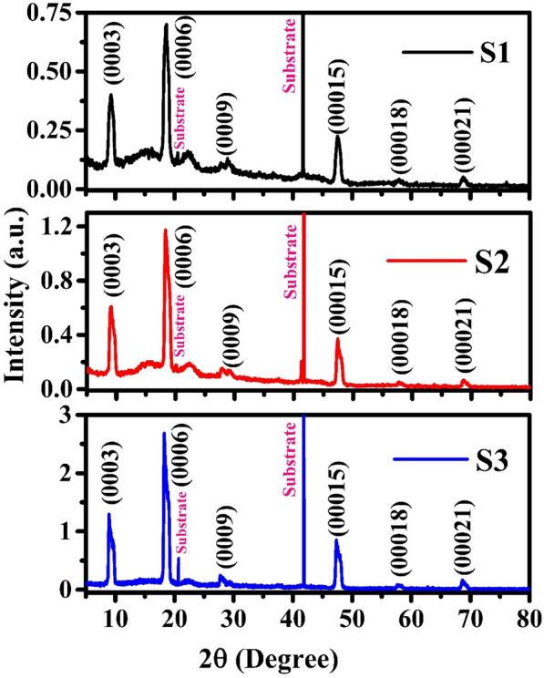
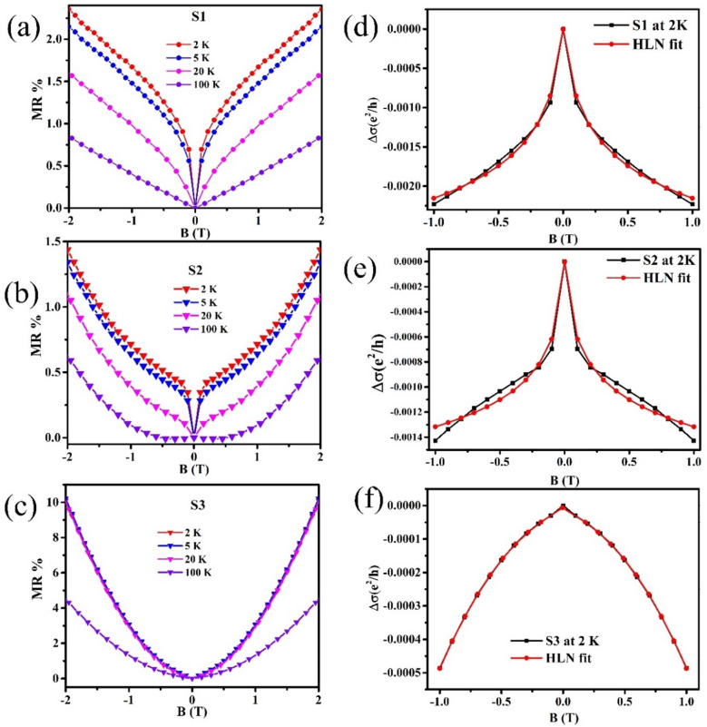
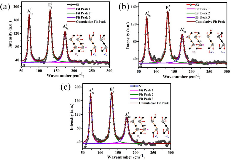
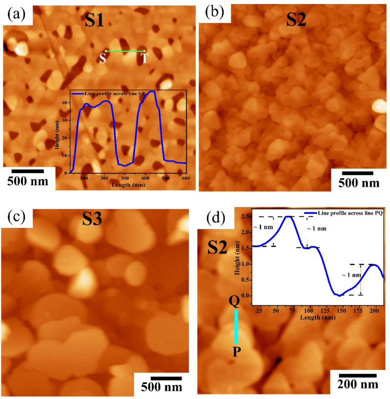
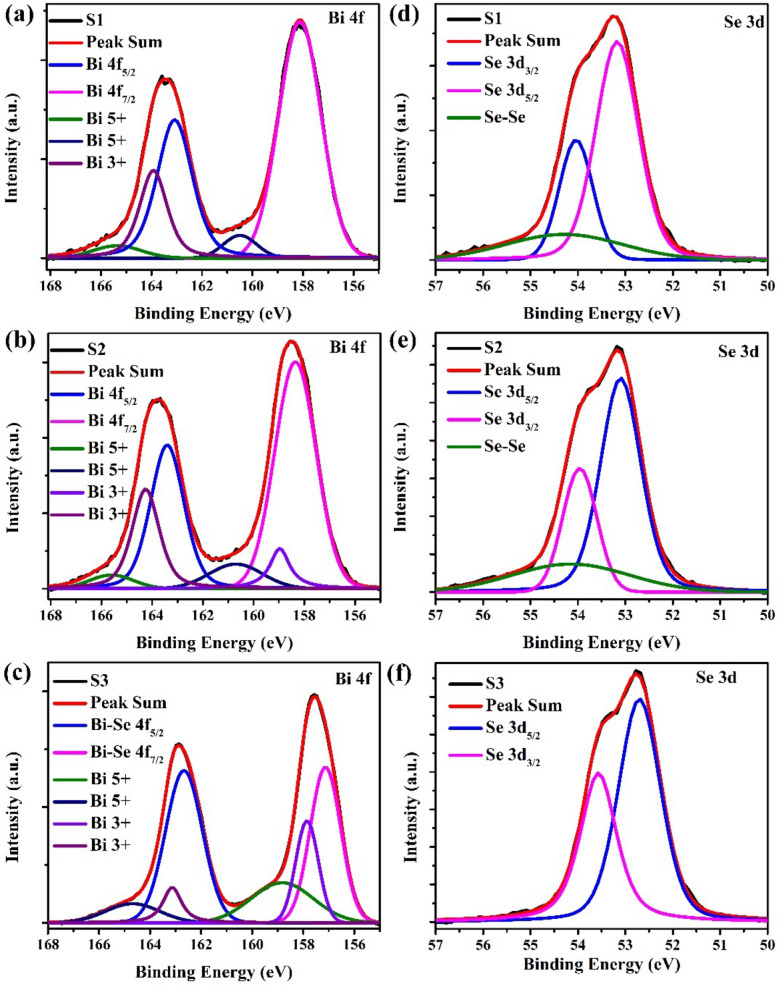
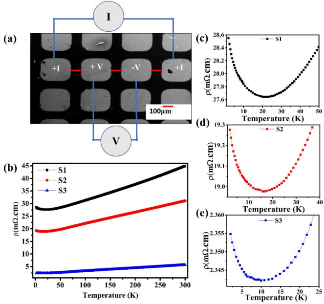
We report a low-temperature magneto transport study of BiSe thin films of different thicknesses (40, 80 and 160 nm), deposited on sapphire (0001) substrates, using radio frequency magnetron sputtering technique. The high-resolution x-ray diffraction measurements revealed the growth of rhombohedral c-axis {0003n} oriented BiSe films on sapphire (0001). Vibrational modes of BiSe thin films were obtained in the low wavenumber region using Raman spectroscopy. The surface roughness of sputtered BiSe thin films on sapphire (0001) substrates were obtained to be ~ 2.26-6.45 nm. The chemical and electronic state of the deposited BiSe was confirmed by X-ray photoelectron spectroscopy and it showed the formation of BiSe compound. Resistivity versus temperature measurements show the metallic nature of BiSe films and a slight up-turn transition in resistivity at lower temperatures < 25 K. The positive magneto-resistance value of BiSe films measured at low temperatures (2-100 K) confirmed the gapless topological surface states in BiSe thin films. The quantum correction to the magnetoconductivity of thin films in low magnetic field is done by employing Hikami-Larkin-Nagaoka theory and the calculated value of coefficient 'α' (defining number of conduction channels) was found to be 0.65, 0.83 and 1.56 for film thickness of 40, 80 and 160 nm, respectively. These observations indicate that the top and bottom surface states are coupled with the bulk states and the conduction mechanism in BiSe thin films varied with the film thicknesses.
我们报道了一项利用射频磁控溅射技术在蓝宝石(0001)衬底上沉积不同厚度(40、80和160纳米)的BiSe薄膜的低温磁输运研究。高分辨率X射线衍射测量表明,在蓝宝石(0001)上生长了菱面体c轴{0003n}取向的BiSe薄膜。利用拉曼光谱在低波数区域获得了BiSe薄膜的振动模式。蓝宝石(0001)衬底上溅射的BiSe薄膜的表面粗糙度约为2.26 - 6.45纳米。通过X射线光电子能谱证实了沉积的BiSe的化学和电子状态,结果表明形成了BiSe化合物。电阻率随温度的测量表明BiSe薄膜具有金属特性,并且在低于25 K的较低温度下电阻率有轻微的上升转变。在低温(2 - 100 K)下测量的BiSe薄膜的正磁电阻值证实了BiSe薄膜中无间隙的拓扑表面态。利用Hikami-Larkin-Nagaoka理论对低磁场下薄膜的磁导率进行了量子修正,对于40、80和160纳米厚的薄膜,计算得到的系数“α”(定义传导通道数)的值分别为0.65、0.83和1.56。这些观察结果表明,BiSe薄膜的顶面和底面状态与体态耦合,并且BiSe薄膜中的传导机制随薄膜厚度而变化。