Cavendish Laboratory, University of Cambridge, 19 J. J. Thomson Avenue, Cambridge, CB3 0HE, U.K.
Materials Science and Engineering, School for Engineering of Matter, Transport and Energy, Arizona State University, Tempe, Arizona 85287, United States.
ACS Nano. 2023 Apr 25;17(8):7326-7334. doi: 10.1021/acsnano.2c10697. Epub 2023 Apr 14.
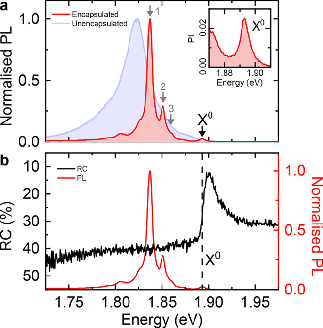
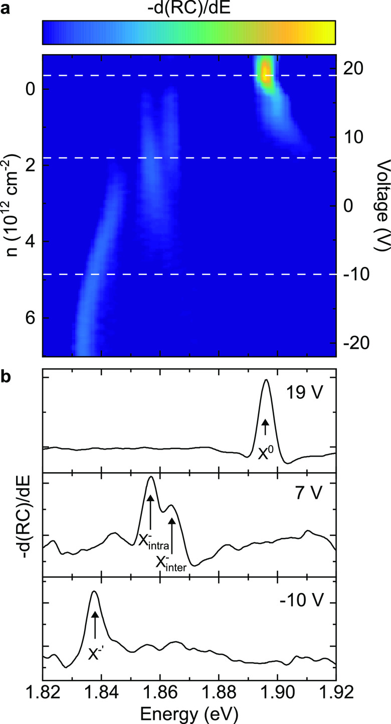
Janus transition-metal dichalcogenide monolayers are artificial materials, where one plane of chalcogen atoms is replaced by chalcogen atoms of a different type. Theory predicts an in-built out-of-plane electric field, giving rise to long-lived, dipolar excitons, while preserving direct-bandgap optical transitions in a uniform potential landscape. Previous Janus studies had broad photoluminescence (>18 meV) spectra obfuscating their specific excitonic origin. Here, we identify the neutral and the negatively charged inter- and intravalley exciton transitions in Janus W monolayers with ∼6 meV optical line widths. We integrate Janus monolayers into vertical heterostructures, allowing doping control. Magneto-optic measurements indicate that monolayer W has a direct bandgap at the K points. Our results pave the way for applications such as nanoscale sensing, which relies on resolving excitonic energy shifts, and the development of Janus-based optoelectronic devices, which requires charge-state control and integration into vertical heterostructures.
Janus 过渡金属二卤族化合物单层是人工材料,其中一个卤族原子平面被不同类型的卤族原子取代。理论预测存在内置的面外电场,从而产生长寿命的偶极激子,同时在均匀的势能景观中保留直接带隙光跃迁。之前的 Janus 研究具有较宽的光致发光(>18meV)光谱,使其特定激子起源变得模糊。在这里,我们在具有约 6meV 光学线宽的 Janus W 单层中识别出中性和带负电荷的谷间和谷内激子跃迁。我们将 Janus 单层集成到垂直异质结构中,从而实现掺杂控制。磁光测量表明,单层 W 在 K 点处具有直接带隙。我们的结果为纳米级传感等应用铺平了道路,这些应用依赖于分辨激子能量位移,以及基于 Janus 的光电设备的发展,这需要电荷态控制和集成到垂直异质结构中。