Department of Electronic Engineering, Hanbat National University, Daejeon, 34158, South Korea.
Radio and Satellite Research Division, Electronics and Telecommunications Research Institute (ETRI), Daejeon, South Korea.
Sci Rep. 2023 Jun 20;13(1):9982. doi: 10.1038/s41598-023-37186-x.
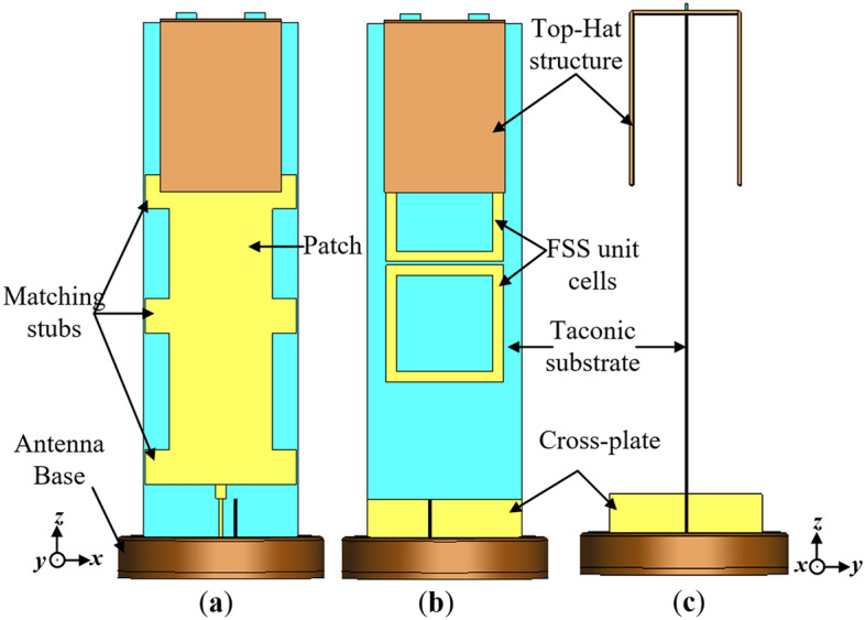
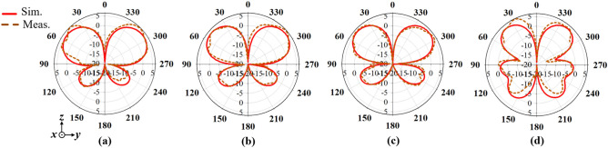
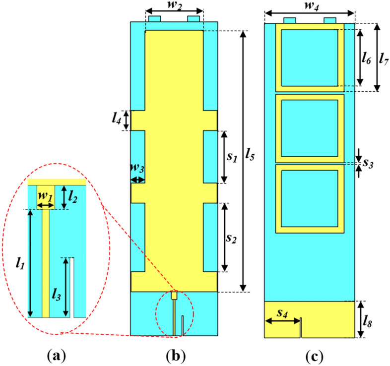
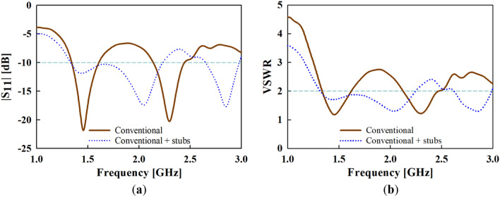
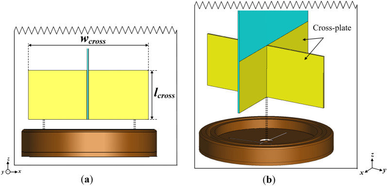
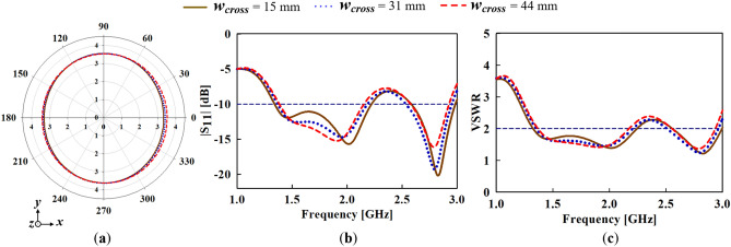
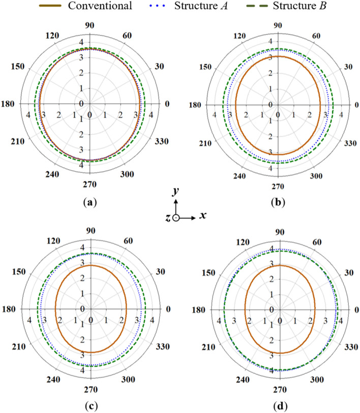
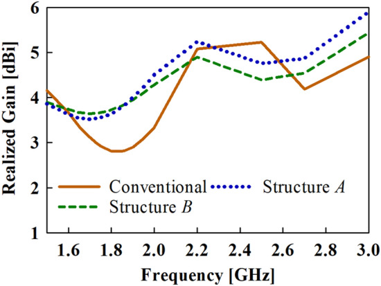
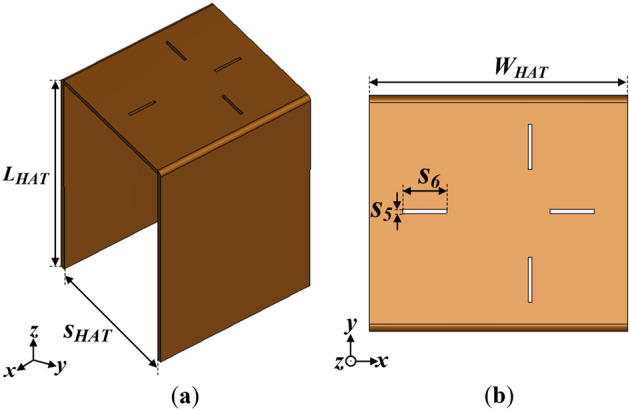
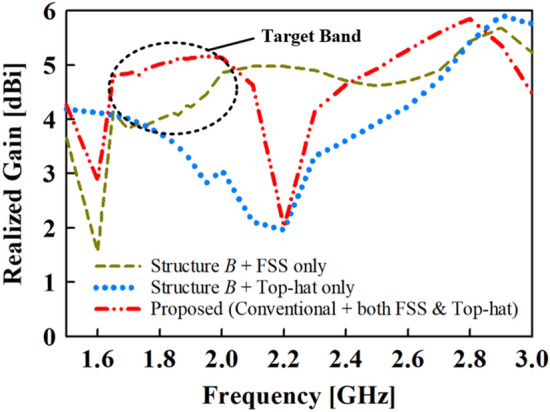
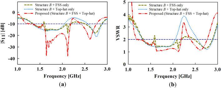
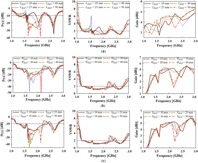
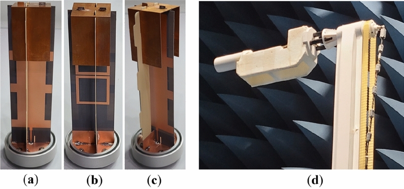
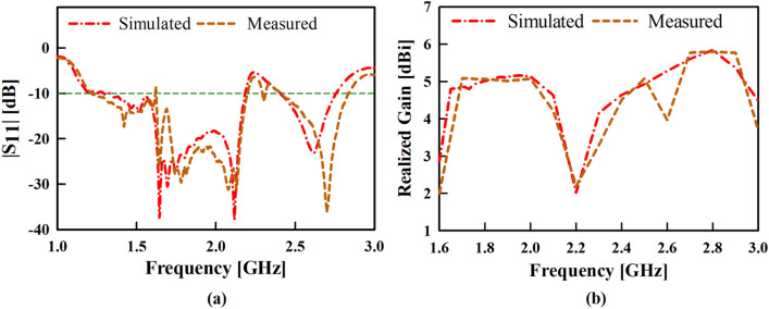
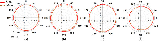
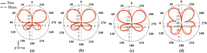
In this paper, a printed monopole antenna with high-gain and dual-band characteristics for applications in wireless local area networks and the internet of things sensor networks is presented. The proposed antenna consists of a rectangular patch with multiple matching stubs surrounded to improve the impedance bandwidth of the antenna. The antenna incorporates a cross-plate structure which is seated at the base of the monopole antenna. The cross-plate consist of metallic plates aligned perpendicularly which enhances the radiations from the edges of the planar monopole to maintain uniform omnidirectional radiation patterns within the antenna's operating band. Furthermore, a layer of frequency selective surface (FSS) unit cells and a top-hat structure is added to the antenna design. The FSS layer consist of three unit cells printed at the back side of the antenna. The top-hat structure is placed on top of the monopole antenna and comprises of three planar metallic structures arranged in a hat-like configuration. The coupling of both the FSS layer and the top-hat structure presents a large aperture to increase the directivity of the monopole antenna. Thus, the proposed antenna structure realizes a high gain without compromising the omnidirectional radiation patterns within the antenna's operating band. A prototype of the proposed antenna is fabricated where good agreement is achieved between the measured and full-wave simulation results. The antenna achieves an impedance bandwidth |S| < - 10 dB and VSWR ≤ 2 for the L and S band at 1.6-2.1 GHz and 2.4-2.85 GHz, respectively. Furthermore, a radiation efficiency of 94.2% and 89.7% is realized at 1.7 and 2.5 GHz, respectively. The proposed antenna attains a measured average gain of 5.2 dBi and 6.1 dBi at the L and S band, respectively.
本文提出了一种应用于无线局域网和物联网传感器网络的具有高增益和双频特性的印刷单极天线。所提出的天线由一个带有多个匹配短截线的矩形贴片组成,以改善天线的阻抗带宽。天线采用十字板结构,位于单极天线的底部。十字板由垂直排列的金属板组成,增强了从平面单极天线边缘的辐射,以保持天线工作频段内的均匀全向辐射模式。此外,在天线设计中添加了一层频率选择表面(FSS)单元和一个顶帽结构。FSS 层由三个单元印刷在天线背面。顶帽结构放置在单极天线的顶部,由三个平面金属结构以帽状形式排列组成。FSS 层和顶帽结构的耦合提供了一个大的孔径,以增加单极天线的方向性。因此,所提出的天线结构在不影响天线工作频段内全向辐射模式的情况下实现了高增益。制作了所提出天线的原型,在测量和全波仿真结果之间取得了良好的一致性。天线在 1.6-2.1GHz 和 2.4-2.85GHz 频段的 L 波段和 S 波段分别实现了 |S| < - 10dB 和 VSWR ≤ 2 的阻抗带宽。此外,在 1.7GHz 和 2.5GHz 时分别实现了 94.2%和 89.7%的辐射效率。所提出的天线在 L 波段和 S 波段的平均增益分别为 5.2dBi 和 6.1dBi。