Zhu Rui, Liang Huili, Liu Shangfeng, Yuan Ye, Wang Xinqiang, Ling Francis Chi-Chung, Kuznetsov Andrej, Zhang Guangyu, Mei Zengxia
Songshan Lake Materials Laboratory, 523808, Dongguan, Guangdong, P. R. China.
Institute of Physics, Chinese Academy of Sciences, 100190, Beijing, P. R. China.
Nat Commun. 2023 Sep 5;14(1):5396. doi: 10.1038/s41467-023-40938-y.
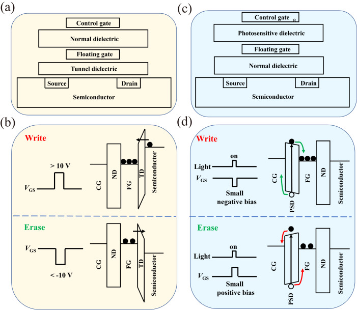
Recently, the optoelectronic memory is capturing growing attention due to its integrated function of sense and memory as well as multilevel storage ability. Although tens of states have been reported in literature, there are still three obvious deficiencies in most of the optoelectronic memories: large programming voltage (>20 V), high optical power density (>1 mW cm), and poor compatibility originating from the over-reliance on channel materials. Here, we firstly propose an optoelectronic memory based on a new photosensitive dielectric (PSD) architecture. Data writing and erasing are realized by using an optical pulse to switch on the PSD. The unique design enables the memory to work with a programming voltage and optical power density as low as 4 V and 160 µW cm, respectively. Meanwhile, this device may be extended to different kinds of transistors for specific applications. Our discovery offers a brand-new direction for non-volatile optoelectronic memories with low energy consumption.
近年来,光电存储器因其传感与存储集成功能以及多级存储能力而受到越来越多的关注。尽管文献中已报道了数十种状态,但大多数光电存储器仍存在三个明显不足:编程电压大(>20 V)、光功率密度高(>1 mW/cm)以及因过度依赖沟道材料而导致的兼容性差。在此,我们首次提出一种基于新型光敏电介质(PSD)架构的光电存储器。通过使用光脉冲开启PSD来实现数据写入和擦除。这种独特设计使该存储器能够分别在低至4 V的编程电压和160 μW/cm的光功率密度下工作。同时,该器件可扩展到用于特定应用的不同类型晶体管。我们的发现为低能耗非易失性光电存储器提供了全新方向。