• 文献检索
  • 文档翻译
  • 深度研究
  • 学术资讯
  • Suppr Zotero 插件Zotero 插件
  • 邀请有礼
  • 套餐&价格
  • 历史记录
应用&插件
Suppr Zotero 插件Zotero 插件浏览器插件Mac 客户端Windows 客户端微信小程序
定价
高级版会员购买积分包购买API积分包
服务
文献检索文档翻译深度研究API 文档MCP 服务
关于我们
关于 Suppr公司介绍联系我们用户协议隐私条款
关注我们

Suppr 超能文献

核心技术专利:CN118964589B侵权必究
粤ICP备2023148730 号-1Suppr @ 2026

文献检索

告别复杂PubMed语法,用中文像聊天一样搜索,搜遍4000万医学文献。AI智能推荐,让科研检索更轻松。

立即免费搜索

文件翻译

保留排版,准确专业,支持PDF/Word/PPT等文件格式,支持 12+语言互译。

免费翻译文档

深度研究

AI帮你快速写综述,25分钟生成高质量综述,智能提取关键信息,辅助科研写作。

立即免费体验

用于低功耗内存计算应用的40纳米分裂栅极NOR闪存器件的设计策略

Design Strategies of 40 nm Split-Gate NOR Flash Memory Device for Low-Power Compute-in-Memory Applications.

作者信息

Yook Chan-Gi, Kim Jung Nam, Kim Yoon, Shim Wonbo

机构信息

Department of Electrical and Information Engineering, Seoul National University of Science and Technology, Seoul 01811, Republic of Korea.

School of Electrical and Computer Engineering, University of Seoul, Seoul 02504, Republic of Korea.

出版信息

Micromachines (Basel). 2023 Sep 7;14(9):1753. doi: 10.3390/mi14091753.

DOI:10.3390/mi14091753
PMID:37763916
原文链接:https://pmc.ncbi.nlm.nih.gov/articles/PMC10537690/
Abstract

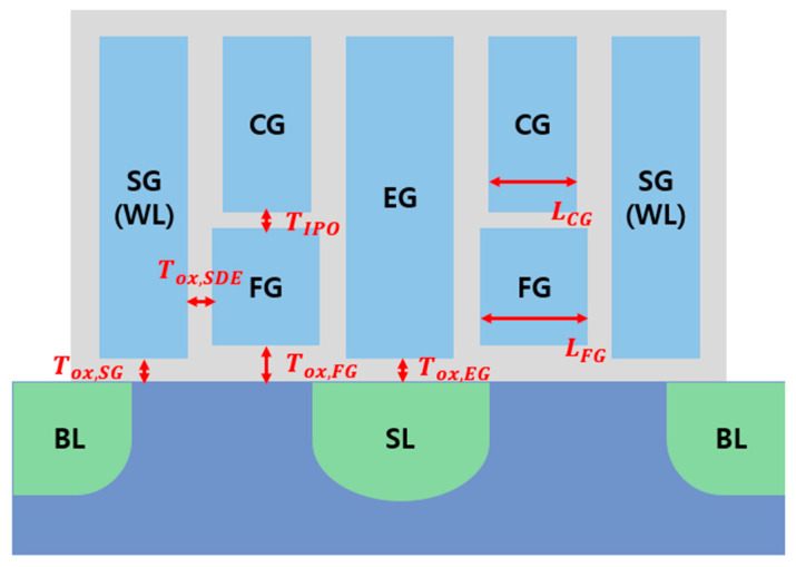
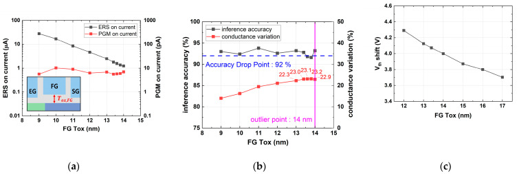
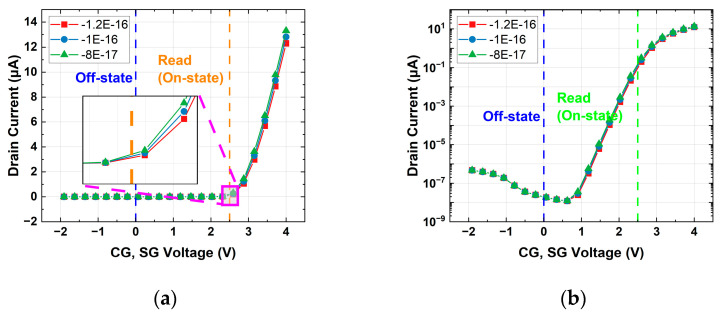
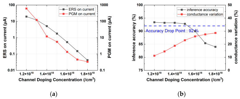
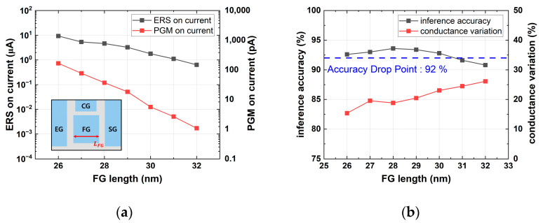
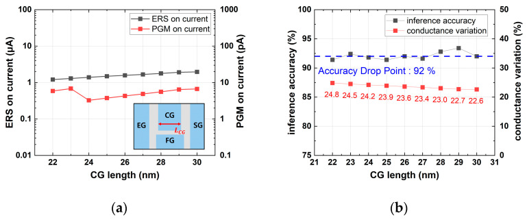
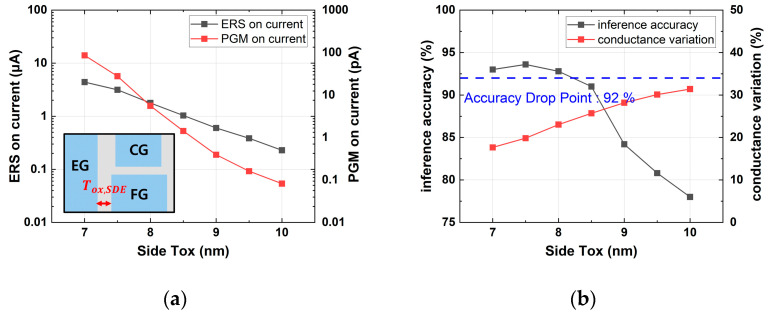
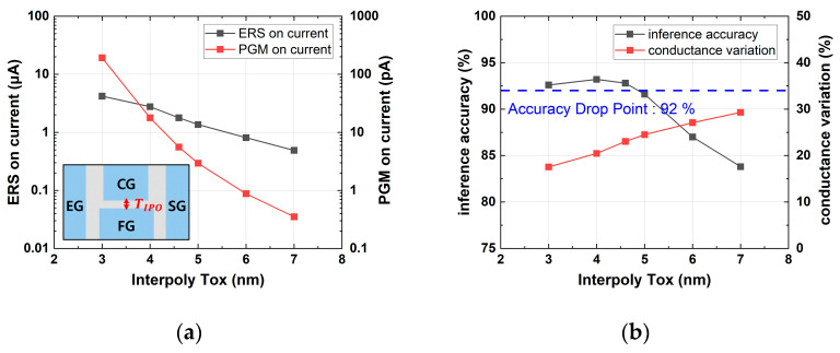
The existing von Neumann architecture for artificial intelligence (AI) computations suffers from excessive power consumption and memory bottlenecks. As an alternative, compute-in-memory (CIM) technology has been emerging. Among various CIM device candidates, split-gate NOR flash offers advantages such as a high density and low on-state current, enabling low-power operation, and benefiting from a high level of technological maturity. To achieve high energy efficiency and high accuracy in CIM inference chips, it is necessary to optimize device design by targeting low power consumption at the device level and surpassing baseline accuracy at the system level. In split-gate NOR flash, significant factors that can cause CIM inference accuracy drop are the device conductance variation, caused by floating gate charge variation, and a low on-off current ratio. Conductance variation generally has a trade-off relationship with the on-current, which greatly affects CIM dynamic power consumption. In this paper, we propose strategies for designing optimal devices by adjusting oxide thickness and other structural parameters. As a result of setting to 13.4 nm, to 4.6 nm and setting other parameters to optimal points, the design achieves erase on-current below 2 μA, program on-current below 10 pA, and off-current below 1 pA, while maintaining an inference accuracy of over 92%.

摘要

现有的用于人工智能(AI)计算的冯·诺依曼架构存在功耗过高和内存瓶颈问题。作为一种替代方案,内存计算(CIM)技术正在兴起。在各种CIM设备候选方案中,分裂栅极NOR闪存具有诸如高密度和低导通状态电流等优点,能够实现低功耗运行,并受益于高度的技术成熟度。为了在CIM推理芯片中实现高能效和高精度,有必要通过在器件层面以低功耗为目标以及在系统层面超越基线精度来优化器件设计。在分裂栅极NOR闪存中,可能导致CIM推理精度下降的重要因素是由浮栅电荷变化引起的器件电导变化以及低开关电流比。电导变化通常与导通电流存在权衡关系,这对CIM动态功耗有很大影响。在本文中,我们提出了通过调整氧化物厚度和其他结构参数来设计最优器件的策略。通过将设置为13.4纳米,设置为4.6纳米并将其他参数设置为最佳点,该设计实现了擦除导通电流低于2微安,编程导通电流低于10皮安,关断电流低于1皮安,同时保持超过92%的推理精度。

https://cdn.ncbi.nlm.nih.gov/pmc/blobs/4007/10537690/59f5d61a0e97/micromachines-14-01753-g010.jpg
https://cdn.ncbi.nlm.nih.gov/pmc/blobs/4007/10537690/1ffe72dbaf62/micromachines-14-01753-g001.jpg
https://cdn.ncbi.nlm.nih.gov/pmc/blobs/4007/10537690/4c51fec24def/micromachines-14-01753-g002.jpg
https://cdn.ncbi.nlm.nih.gov/pmc/blobs/4007/10537690/b21f80d205cc/micromachines-14-01753-g003.jpg
https://cdn.ncbi.nlm.nih.gov/pmc/blobs/4007/10537690/6fc731ca6d23/micromachines-14-01753-g004.jpg
https://cdn.ncbi.nlm.nih.gov/pmc/blobs/4007/10537690/06b2a3d550b5/micromachines-14-01753-g005.jpg
https://cdn.ncbi.nlm.nih.gov/pmc/blobs/4007/10537690/4ea5523f3106/micromachines-14-01753-g006.jpg
https://cdn.ncbi.nlm.nih.gov/pmc/blobs/4007/10537690/9b8d947759d6/micromachines-14-01753-g007.jpg
https://cdn.ncbi.nlm.nih.gov/pmc/blobs/4007/10537690/26eacd86f07f/micromachines-14-01753-g008.jpg
https://cdn.ncbi.nlm.nih.gov/pmc/blobs/4007/10537690/252f6c023552/micromachines-14-01753-g009.jpg
https://cdn.ncbi.nlm.nih.gov/pmc/blobs/4007/10537690/59f5d61a0e97/micromachines-14-01753-g010.jpg

相似文献

1
Design Strategies of 40 nm Split-Gate NOR Flash Memory Device for Low-Power Compute-in-Memory Applications.用于低功耗内存计算应用的40纳米分裂栅极NOR闪存器件的设计策略
Micromachines (Basel). 2023 Sep 7;14(9):1753. doi: 10.3390/mi14091753.
2
Simulation of a Fully Digital Computing-in-Memory for Non-Volatile Memory for Artificial Intelligence Edge Applications.用于人工智能边缘应用的非易失性存储器全数字内存计算模拟
Micromachines (Basel). 2023 May 31;14(6):1175. doi: 10.3390/mi14061175.
3
A compute-in-memory chip based on resistive random-access memory.基于电阻式随机存取存储器的计算内存芯片。
Nature. 2022 Aug;608(7923):504-512. doi: 10.1038/s41586-022-04992-8. Epub 2022 Aug 17.
4
FinFET 6T-SRAM All-Digital Compute-in-Memory for Artificial Intelligence Applications: An Overview and Analysis.用于人工智能应用的FinFET 6T-SRAM全数字内存计算:概述与分析
Micromachines (Basel). 2023 Jul 31;14(8):1535. doi: 10.3390/mi14081535.
5
SRAM-Based CIM Architecture Design for Event Detection.基于静态随机存储器的事件检测 CIM 体系结构设计。
Sensors (Basel). 2022 Oct 16;22(20):7854. doi: 10.3390/s22207854.
6
Double-Gate MoS Field-Effect Transistor with a Multilayer Graphene Floating Gate: A Versatile Device for Logic, Memory, and Synaptic Applications.双层门控 MoS 场效应晶体管与多层石墨烯浮栅:用于逻辑、存储和突触应用的多功能器件。
ACS Appl Mater Interfaces. 2020 Jul 29;12(30):33926-33933. doi: 10.1021/acsami.0c08802. Epub 2020 Jul 20.
7
Dielectric-Engineered High-Speed, Low-Power, Highly Reliable Charge Trap Flash-Based Synaptic Device for Neuromorphic Computing beyond Inference.用于超越推理的神经形态计算的介电工程高速、低功耗、高可靠的基于电荷陷阱闪存的突触器件。
Nano Lett. 2023 Jan 25;23(2):451-461. doi: 10.1021/acs.nanolett.2c03453. Epub 2023 Jan 13.
8
Future prospects of NAND flash memory technology--the evolution from floating gate to charge trapping to 3D stacking.NAND闪存技术的未来前景——从浮栅到电荷俘获再到3D堆叠的演进
J Nanosci Nanotechnol. 2012 Oct;12(10):7604-18. doi: 10.1166/jnn.2012.6650.
9
3D NAND Flash Memory Based on Double-Layer NC-Si Floating Gate with High Density of Multilevel Storage.基于具有高密度多级存储的双层非晶硅纳米晶硅浮栅的3D NAND闪存。
Nanomaterials (Basel). 2022 Jul 18;12(14):2459. doi: 10.3390/nano12142459.
10
Compute in-Memory with Non-Volatile Elements for Neural Networks: A Review from a Co-Design Perspective.基于协同设计视角的神经网络非易失性元件内存计算综述
Adv Mater. 2023 Sep;35(37):e2204944. doi: 10.1002/adma.202204944. Epub 2023 Mar 2.

本文引用的文献

1
Accurate deep neural network inference using computational phase-change memory.利用计算相变化内存实现精确的深度神经网络推理。
Nat Commun. 2020 May 18;11(1):2473. doi: 10.1038/s41467-020-16108-9.