Ghosh Mandira, Mukherjee Debdyuti, Selvaraj Celin, Ghosh Pritam, Sarkar Sujoy
Department of Chemistry, School of Advanced Sciences, Vellore Institute of Technology, Chennai Campus, Vandalur-Kelambakkam Road, Chennai, Tamil Nadu 600127, India.
Centre for Fuel Cell Technology (CFCT), International Advanced Research Centre for Powder Metallurgy and New Materials (ARCI), IIT-M Research Park, Taramani, Chennai 600113, India.
ACS Omega. 2024 Dec 8;9(52):51136-51145. doi: 10.1021/acsomega.4c06548. eCollection 2024 Dec 31.
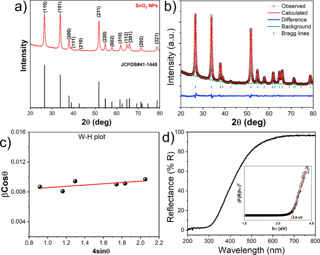
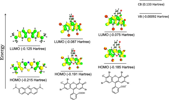
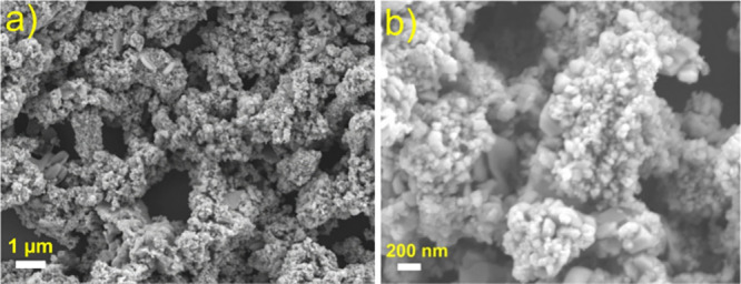
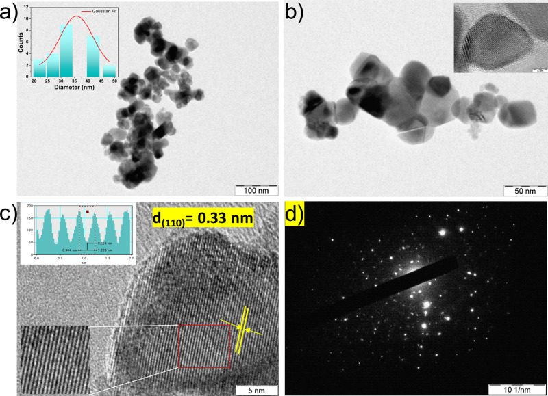
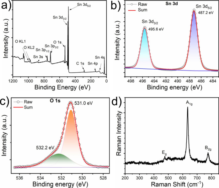
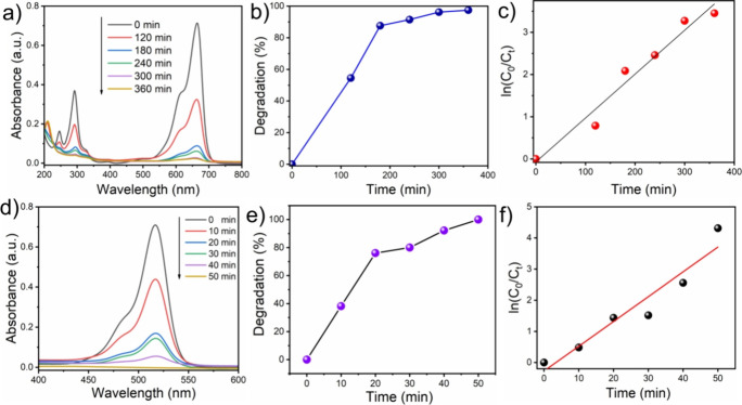
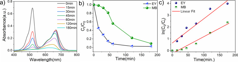
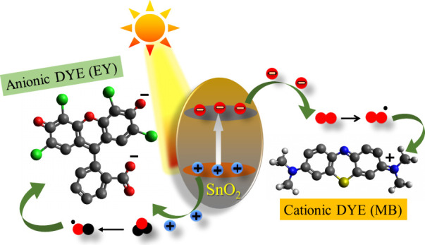
Electronic waste (e-waste) has become a significant environmental concern worldwide due to the rapid advancement of technology and short product lifecycles. Waste-printed electronic boards (WPCBs) contain valuable metals and semiconductors; among them, tin can be recycled and repurposed for sustainable material production. This study presents a potential ecofriendly methodology for the recovery of tin from WPCBs in the form of tin oxide nanostructured powders. The soldering points in the WPCBs are extracted and dissolved in the dilute HNO solution, followed by the formation of metastannic acid, which is subsequently transformed into SnO nanoparticles. Different characterization techniques (XRD, XPS, FE-SEM, and TEM) are employed to confirm the morphology and composition of nanoparticles. The prepared SnO NPs, having a size range of <50 nm, show excellent photocatalytic degradation of cationic (methylene blue, MB) and anionic (eosin Y, EY) dyes for wastewater treatment. The as-synthesized SnO can degrade the mixed dyes (MB+EY) under the illumination of natural sunlight at rate constants of 0.0153 and 0.1103 min for MB and EY, respectively. The positive zeta potential and smaller particle size of the SnO NPs possess the extra advantage of the adsorption of anionic over cationic dye, resulting in faster degradation of EY, which is further supported by DFT calculation. The synthesis of SnO from waste-printed electronic boards offers a dual benefit: It not only provides a sustainable solution for managing electronic waste but also contributes to the production of useful photocatalysts for wastewater treatment. By converting waste into valuable resources, this approach aligns with the principles of the circular economy and mitigates the environmental impact associated with e-waste disposal.
由于技术的快速发展和产品生命周期的缩短,电子废物(电子垃圾)已成为全球一个重大的环境问题。废弃印刷电路板(WPCBs)含有有价值的金属和半导体;其中,锡可以回收并重新用于可持续材料生产。本研究提出了一种潜在的生态友好方法,用于以氧化锡纳米结构粉末的形式从WPCBs中回收锡。提取WPCBs中的焊点并将其溶解在稀硝酸溶液中,随后形成偏锡酸,偏锡酸随后转化为SnO纳米颗粒。采用不同的表征技术(XRD、XPS、FE-SEM和TEM)来确认纳米颗粒的形态和组成。制备的尺寸范围小于50nm的SnO纳米颗粒对用于废水处理的阳离子(亚甲基蓝,MB)和阴离子(曙红Y,EY)染料表现出优异的光催化降解性能。合成的SnO在自然阳光照射下可以降解混合染料(MB+EY),MB和EY的降解速率常数分别为0.0153和0.1103min⁻¹。SnO纳米颗粒的正zeta电位和较小的粒径具有吸附阴离子染料优于阳离子染料的额外优势,导致EY降解更快,这得到了密度泛函理论计算的进一步支持。从废弃印刷电路板合成SnO有双重好处:它不仅为管理电子废物提供了可持续的解决方案,还为废水处理生产有用的光催化剂做出了贡献。通过将废物转化为有价值的资源,这种方法符合循环经济的原则,并减轻了与电子废物处理相关的环境影响。